I just destroyed a circuit I spent over a week preparing and I decided I would learn how to better protect my circuits.
Reverse Polarity protection:
A diode can be used to protect a circuit but it will drop 0.7V and will waste power. A shotky diode will only drop .3-.4V but it has the same issue. A P-Channel MOSFET set up where the gate is connected to ground will only turn on when the polarity is correct. If Vin is not greater than the maximum allowed voltage you can put accross the MOSFET from gate to source (Vgs max.), or the Vin is not less than the threshold required for the P-FET to turn on (Vgs th), then it doesn’t need any other components.
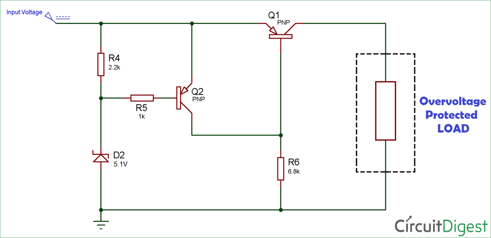
For overvoltage protection (https://circuitdigest.com/electronic-circuits/overvoltage-protection-circuit):
When the voltage is below the Zener Diode’s 5.1V reverse threshold, Q2’s base is HIGH (through the 2.2K resistor) so the PNP is off. This means that Q1 is ON (because it’s PNP base is connected to ground via 6.8K) and the circuit is powered.
When the voltage is above the Zener Diode’s 5.1V reverse threshold, Q2 is connected to ground and is turned on. This connects Q1 with VCC and therefore turns it off, disconnecting the circuit from the power.
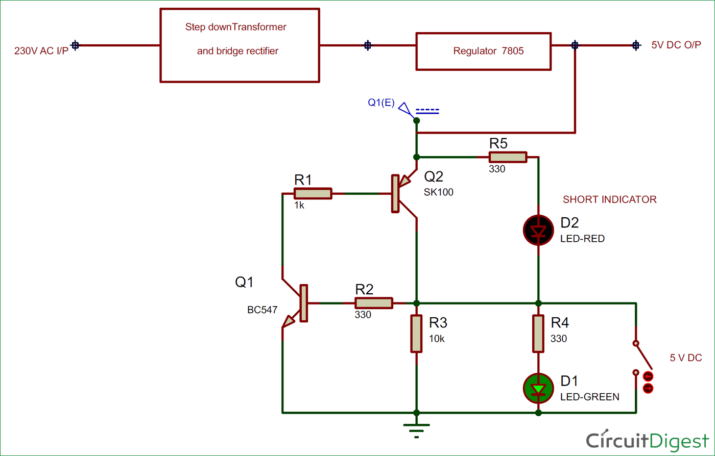
For short circuit protection:
Q2 is a PNP, Q1 is an NPN. Here is my understanding based on the site https://circuitdigest.com/electronic-circuits/short-circuit-protection-circuit-diagram
First a small amount of current reaches the base of Q1 (via R5 and the D2), causing it to turn on Q2. Now current flows through Q2 into R4 and D1 while keeping Q1 on. Current is no longer flowing through D2.
When a short occurs, current passes directly towards ground from Q2 and therefore no longer turns Q1 on. This turns off Q2 and now current passes via R5 and D2, skipping D1 and still skipping R2 towards Q1, directly to ground. Instead of having a short, we now have current passing through R5 and D2.
PCB Design (from https://www.youtube.com/watch?time_continue=5&v=NJKZZArjdg8&feature=emb_logo):
-rounded corner for logic levels, straight corners “round edges”. (Though not everyone seems to agree on this). 45 degree angles are good, 90 are bad.
-minimize trace lengths, components electronically close should be physically close too. Longer traces have higher resistance, capacitance and inductance.
-Think in terms of a signal chain, with input on the left moving towards output on the right. Divide things into building blocks. Build each block separately and then throw it on the main board.
-VCC should be connected via a star-like formation to sub systems, with branches of equal length, NOT in a cascaded or serial way where the last sub system is furthest away from VCC. This will make the later sub systems vulnerable to noise produced by the upstream ones.
-Mechanical parts (pots, switches, barrel connectors) fail before electrical parts.
-watch out for your ground returns (the path that a component’s ground path with take to make it back to the power regulator). If it is zig zaggy and not short this is not ideal.
-don’t forget to add test points!
This website helps to calculate the correct width of traces for a given current:
http://circuitcalculator.com/wordpress/2006/01/31/pcb-trace-width-calculator/
This resource looks good for more in depth: http://alternatezone.com/electronics/files/PCBDesignTutorialRevA.pdf
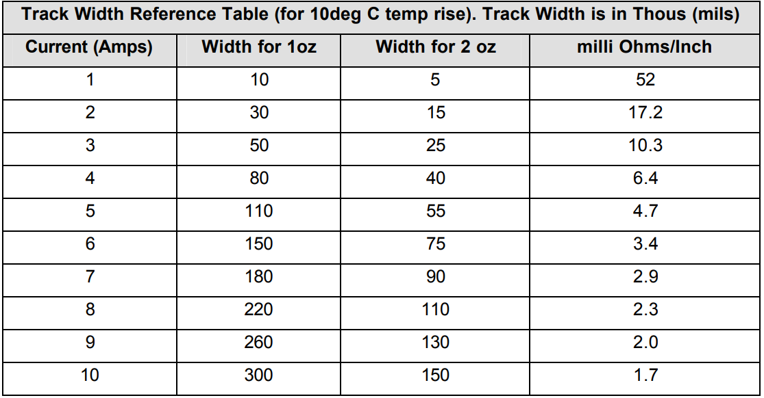
Here is a table showing minimum trace widths for different thicknesses of copper:
 •••••••••••••••
-work in mils, most components are designed with 100 mil spacing (0.1″).
-For your Eagle grid, had a 25 thou alt grid with a 50 thou main grid. Or a 25mil/10mil for finer work. Use a SNAP grid.
-bigger traces are better generally, they have lower DC resistance and lower inductance.
-25 thou for signal traces, 50 thou for power, 10-15 for traces going in between ICs is a good place to start.
-oval shaped pads for ICs, circular for leaded resistors and caps.
-minimize the number of drill bits that will be required by the board house to make your circuit.
-check that when you actually add the components, screws, etc., it all fits and doesn’t cause potential shorts.
-do not mix analog and digital sub systems in the same circuit, nor high current or frequency and low current and frequency.
-leave a rectangle at the top of the solder mask so you can write something in pen on the board!
-for a two sided board, the bottom can be a ground plane. You should not have the ground plane extend all the way to the edge of the board. The more copper in your ground path the lower the impedance.
-Use multiple vias to connect the same signal to ground to lower impedance.
-One bypass cap per IC: 10nF or 1nF for higher frequencies, and 1uF or 10uF for low frequencies
-boards are typically made with 1oz. copper thickness and are 1.6mm thick fiberglass FR4.
-don’t forget to add a signature/logo to your board!
Visualizing your circuit before building:
https://www.falstad.com/circuit/