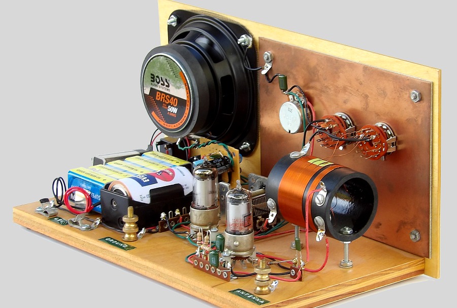
Inspired by the history of mounting circuits on wood with screws and wire, evoking John Cage’s prepared pianos.
This iteration of the project is born of a few realizations :
- VGA is an analog signal, it’s not digital.
- The coolest effects are the simplest ones : XOR, HP and LP filters, comparators, etc. which can be easily made with discrete components.
- A simple low frequency oscillator could control these effects with an LED > LDR voltage controlled resistor set-up.
- Two out of sync oscillators easily make a pattern that doesn’t repeat often and is difficult to predict.
Pedagogically and aesthetically I like this idea : it goes back to the basics of electronics, the history of electronics, and will show the materiality of video signals. This in contrast to the overly complex use of digital components to do basic modifications…
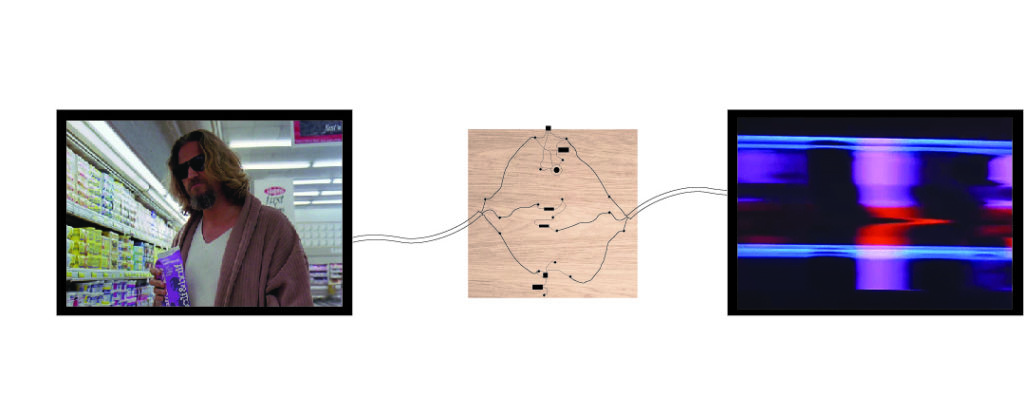
The three basic circuits :
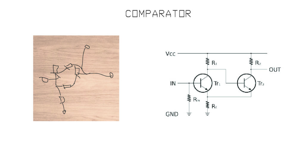
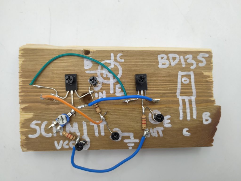
*TESTED* This works (powered at 5V, with pull down 10K on input and the rest 1K and two BD135s) at lower frequencies (<100KHz) around 5V. I added a 5K variable resistor (or an LDR + resistor) to increase the resistance of R1 and it varies the threshold !
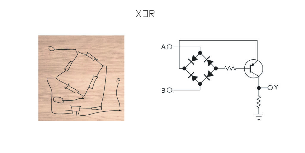
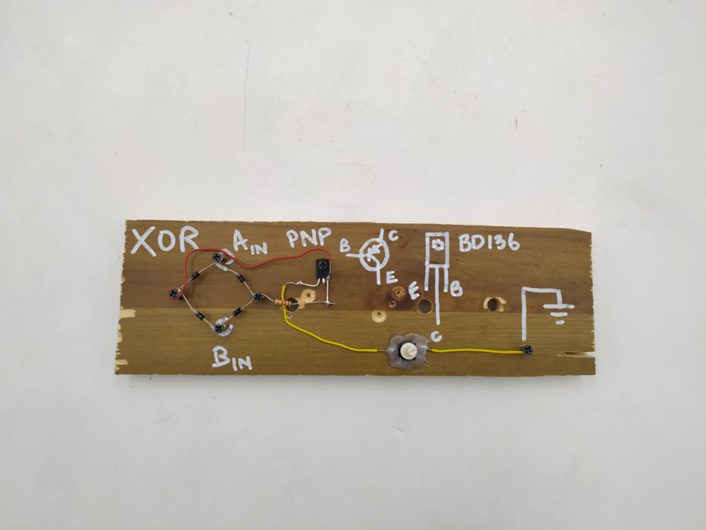
*TESTED* Works using BD136 PNP, 10K for the pull down and 1K for the base protection. General purpose diodes. I replaced the pull down with a 5K variable resistor and got some messed up results in the MHz. Doesn’t need power – just takes it from the input signal ! (But VGA signal would need to be amplified in order to work.
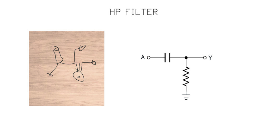
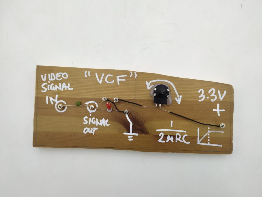
*TESTED* With a 104 cap and 5K variable resistor I can vary the filtering of a 5V function generator signal.
****
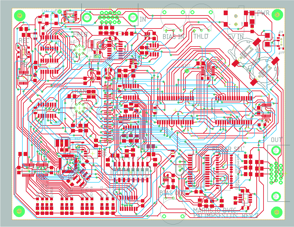
OK we’re back to the original plan ! Here is the Palimsest.OS Rev.2 :
WHY ?
- This board is for the inauguration of the IFT at the DVIC. It has to demonstrate technical proficiency on behalf of the staff, and must run independently as an tech-art installation, modifying video independently day in day out.
- Rev.1 didn’t work for microchip automation, this one should work smoothly(?). If everything works I could write code that executes different video manipulations. I also added selection LEDs to show the microchip doing its thing.
- This tests the 8 channel 1-bit WRITE/REWRITE memory idea (but not the more elegant SRAM + buffer idea of Fabien), with certain effects tied to certain channels
- Incorporates a simple to control XOR, comparator and HP/LP/BP filter into one board
- Has a stable clock setup with metal can oscilloscope, a gen lock IC, and V SYNC burst setup
- Tests an (expensive) programmable filter IC
- It is a test for a simpler, inexpensive 8 ch recorder board that could be a cool kit
- Does away with the ADC and all its pesky issues and trades it for a simpler 1bit “ADC”.
- I’m also using 5V SRAM to avoid the headache of different logic levels (though this means I only have 4MB of SRAM versus 16MB).
- For testing purposes it can be soldered as a logic-controlled board or as a physical switch controlled-board.
- Instead of having lots of jumpers for wires, I went for rotary switches to make things more plug and play. However this also means that there are fewer experminental tests that are facilitated (like disabling a single counter while recording etc.) that were possible on rev.1
- Can layer different recorded portions easily in theory
- Battery switch and edge potentiometers instead of knobs
- Theoretically could do feedback and echo tests with this board as it can read and write from and into memory simoultaneously
- This board should be easier to work with than the previous stacked PCI-E motherboard design which made knob turning and mounting hard.
- Instead of using generic octal logic ICs I went for more specific purpose ones.
- The board will be made at https://aisler.net/ instead of JLCPCB so I’m hoping for a really nice finish
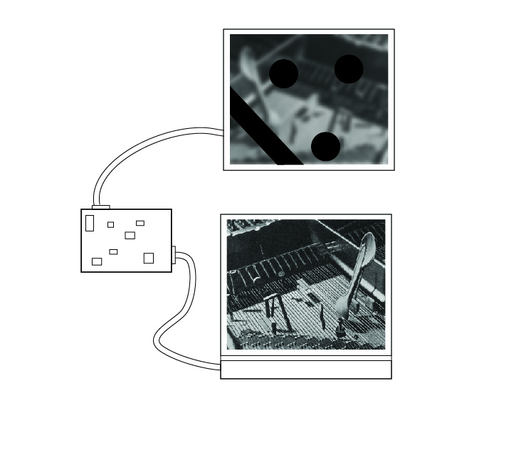
Here’s a possible minimal installation with it :
****
PALIMPSEST.OS v2 ERRATA :
- Pin 1 of the 40MHz clock should be pulled HIGH to be enabled, not LOW as it is on the board !
- The THRESHOLD pot isn’t connected to GND on one side…
- I should have tied the CCLR (pin 10, which resets when pulled LOW) of the 590 to VCC with a 10K instead of leaving it floating connected to VSYNC. This made it malfunction.
- BIG PROBLEM : I ordered multiplexers (unidirectional) instead of analog switches (bidirectional) ! The ‘157 multiplexers mess with SRAM B’s I/Os when it is in READ mode (when the SRAM is outputing values on the I/O pins). I ordered a replacement that is pin compatible, the 74LVC1G3157 (DATASHEET : https://www.ti.com/lit/ds/symlink/sn74lvc1g3157.pdf?HQS=dis-mous-null-mousermode-dsf-pf-null-wwe&ts=1679316452048&ref_url=https%253A%252F%252Fwww.mouser.de%252F). EDIT* The new components work perfectly – everything is good !
- The Sync Clock IC is 3.3V not 5V…
- Image jumps around of course. When I try to record with the Burst AND IC which outputs !CLK, no writing can occur. I’m guessing this gate messes with the timing somehow? As a workaround I’m trying to connect the 4 AND’ed V SYNC counts to either the address counter IC Reset or to another reset somewhere.
- Lots of noise on V SYNC, I should maybe have made the input and output VGA jacks right next to one another…
- Pin 9 of the VGA D-SUB 15 is VCC for the Display ID EEPROM chip – but I have it connected to GND !! In general I need to respect the rules around the different grounds and return pins in the VGA protocol and not just connect them all together. Hoping to fix this in the next version.
More Meta errata :
- It’s a bit muddy with several channels, would be cool to be able to filter that
- I need a path to feedback with a pot !
- Switched the output resistors to a 150ohm going to R,G,B and it works nicely.
- Dip switch hard to use without tool.
- Hard to see which direction switches are pointing in darker light
Oy vey ! I realized that I could just use an I2C RAM IC and save about a billion components. Here are the more plug and play simple boards I made in the aftermath :
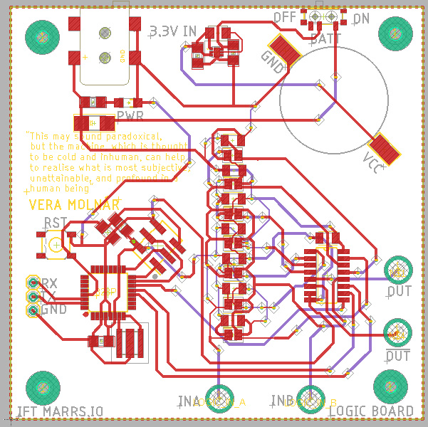
Good news: The 328 works.
ERRATA : I fried the logic chips with 5V :(. Resoldered new ones and looks good. I think I need to be feeding in a signal that has already been digitized (like by a comparator). Otherwise I need to mess around with knobs to get the signal right around the threshold of the logic gates with bias setup.
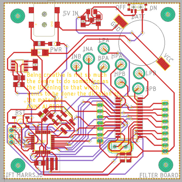
Good news: The 328 works. And I can see the effect of selecting different filters. I’m not sure why but it works best when the signal is coming in on A and I’m taking the output on B (or vice versa). I’ve also got a cap going from the output of the filter board before amplifying it again.
ERRATA: I ordered the wrong length of bussed resistor network.
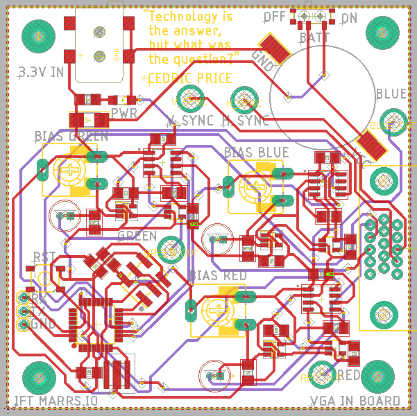
Good news: The 328 works.
errata ^ Wrong footprint (and value!) for the digital potentiometer here… Will have to wait for the correct part to test this.
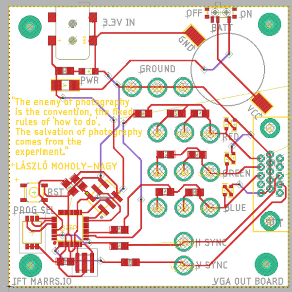
Good news: The 328 works and at least it produces an image !
errata ^ H SYNC and V SYNC plugged in to wrong pins on Arduino (should be PD3 and PB1 respectively).
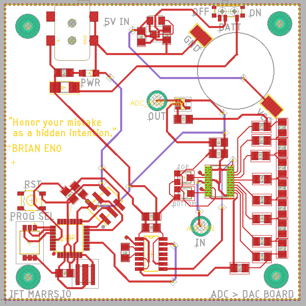
Good news: The 328 works.
ERRATA : the PD pin (which enables ADC IOs when low) is pulled HIGH ! I resoldered it and now it’s working great.
I chose a non PWM pin on the atmega to be the voltage control pin of the VCO… I soldered it to the nextdoor pin which can do PWM and all is good.
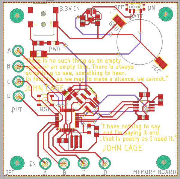
ERRATA: I tried two chips, they both come up as unidentified FRAM when I have them speak on the serial running the demo codes…I should probably pull Write Protect (WP) HIGH just in case. Still not working…I will try replacing with a 23LC1024 serial SPI SRAM as it has the same pinout.
***EDIT: Just saw this on the Adafruit website : “For the 4Mbit version, you should change this to: fram.begin(3)”…Still doesn’t work though.
I replaced with the 23LC1024 and am using the SRAMsimple libary which appears to work well. For some reason the digitalRead I’m doing in the setup is always returning 0 even if connected to 5V.
#include <SRAMsimple.h>
#defineCSPIN8       // Default Chip Select Line for Uno (change as needed)
SRAMsimple sram;       //initialize an instance of this class
/*******  Set up code to define variables and start the SCI and SPI serial interfaces  *****/
voidsetup()
{
uint32_t address = 0;                       // create a 32 bit variable to hold the address (uint32_t=long)
Serial.begin(9600);                         // set communication speed for the serial monitor
SPI.begin();                                // start communicating with the memory chip
  // And now the fun begins:
/**********Write a Single Byte *******************/
bool data = digitalRead(A0);                        // initialize the data
for(int i = 0; i <=5; i++){                 // Let's write 5 individual bytes to memory
    address = i;                              // use the loop counter as the address
sram.WriteByte(address, byte(data));            // now write the data to that address
    data+=2;                                  // increment the data by 2
}
/********* Read a single Byte *********************/
Serial.println("Reading each data byte individually: ");
  byte value;                                 // create variable to hold the data value read
for(int i = 0; i <=5; i++){                 // start at memory location 0 and end at 5
    address = i;                              // use the loop counter as the memory address
    value = sram.ReadByte(address);           // reads a byte of data at that memory location
Serial.println(value);                    // Let's see what we got
}
}
Not sure why…
*EDIT: Got the thing working with Fabien’s help !
#include <SPI.h>
#include <SRAM_23LC.h>
#define SPI_PERIPHERAL SPI
#define CHIP_SELECT_PIN 8

SRAM_23LC SRAM(&SPI_PERIPHERAL, CHIP_SELECT_PIN, SRAM_23LC1024);

#define START_ADDRESS 0

void setup(void)
{
pinMode(2, OUTPUT); // where we write the recorded data to.
pinMode(A2, INPUT);
SRAM.begin();
}

void loop(void)
{
for(unsigned long i=0; i<128000; i++)
{
byte val;
if ( (PINC & (1 << PINC2)) == (1 << PINC2) ) {
val = 255; // pin is high
}
else {
val = 0; // pin is low
}
SRAM.writeByte(START_ADDRESS + i, val);
}

delayMicroseconds(1);

for(unsigned long i=0; i<128000; i++)
{
byte ch = SRAM.readByte(START_ADDRESS + i);
PORTD = ch;
}

delayMicroseconds(1);
}
However in this byte write/read mode the fastest I can get it going is 10KHz…The next step is to use this SPI tutorial (https://docs.arduino.cc/tutorials/generic/introduction-to-the-serial-peripheral-interface) and the SRAM datasheet ( https://ww1.microchip.com/downloads/aemDocuments/documents/MPD/ProductDocuments/DataSheets/23A1024-23LC1024-1-Mbit-SPI-Serial-SRAM-with-SDI-and-SQI-Interface-DS20005142.pdf) to operate in “sequential operation” mode where pages are ignored and its all just one big array.
I have tried to do this but haven’t yet succeeded. I can successfully write and read from the memory with the code below..:
#define DATAOUT 11//MOSI
#define DATAIN 12//MISO
#define SPICLOCK 13//sck
#define CHIPSELECT 8//ss

//opcodes
#define READ 0x03 // read data
#define WRITE 0x02 // write data
#define WRMR 0x01 // write to the Mode Register

//modes
#define SEQUENTIAL 0x20 // 0100000 in Binary

byte clr;

byte address0 = 0;
byte address1 = 0;
byte address2 = 0;

byte data_to_write = 0;
byte data_to_read = 0;

char spi_transfer(volatile byte data)
{
SPDR = data; // Start the transmission
while (!(SPSR & (1<<SPIF))) // Wait the end of the transmission
{
};
return SPDR; // return the received byte
}

void setup(void)
{

pinMode(DATAOUT, OUTPUT);
pinMode(DATAIN, INPUT);
pinMode(SPICLOCK,OUTPUT);
pinMode(CHIPSELECT,OUTPUT);
digitalWrite(CHIPSELECT,HIGH); //disable device
pinMode(2, OUTPUT); // where we write the recorded data to.
//pinMode(10, OUTPUT); // LED
pinMode(A2, INPUT); // where we read the data from
// SPCR = 01010000
//interrupt disabled,spi enabled,msb 1st,controller,clk low when idle,
//sample on leading edge of clk,system clock/4 rate (fastest)
SPCR = (1<<SPE)|(1<<MSTR);
clr=SPSR;
clr=SPDR;

digitalWrite(CHIPSELECT,LOW);
spi_transfer(WRMR); // access the Mode Register
spi_transfer(SEQUENTIAL);//enter Sequential Mode
digitalWrite(CHIPSELECT,HIGH); //disable device
}
void loop(void)
{
//WRITE
digitalWrite(CHIPSELECT,LOW);
spi_transfer(WRITE);
spi_transfer(address0);
spi_transfer(address1);
spi_transfer(address2);

for(unsigned long i=0; i<128000; i++) // address is automatically incremented internally in the SRAM in this mode
{
if ( (PINC & (1 << PINC2)) == (1 << PINC2) ) {
data_to_write = 255; // pin is high
}
else {
data_to_write = 0; // pin is low
}
spi_transfer(data_to_write);
}
digitalWrite(CHIPSELECT,HIGH);

//READ
digitalWrite(CHIPSELECT,LOW);
spi_transfer(READ); //transmit read opcode
spi_transfer(address0);
spi_transfer(address1);
spi_transfer(address2); // 24 bit address in three parts (this could be a problem)

for(unsigned long i=0; i<128000; i++)
{
data_to_read = spi_transfer(0xFF); //get data byte
PORTD = data_to_read;
}
digitalWrite(CHIPSELECT,HIGH); //release chip, signal end transfer
}
…but when I do this in chunks with loops it doesn’t appear to work. I’m not sure if it’s because I’m reading the value of the pin during the writing and if I should perhaps do this before with a buffer array and then just read from it ?
OVERALL ERRATA : I also need some kind of power board that distributes 5V and 3.3V
***
On the back of the boards I tried an experiment using the bmp import ULP in Eagle. Not sure what the results will look like :
 An
An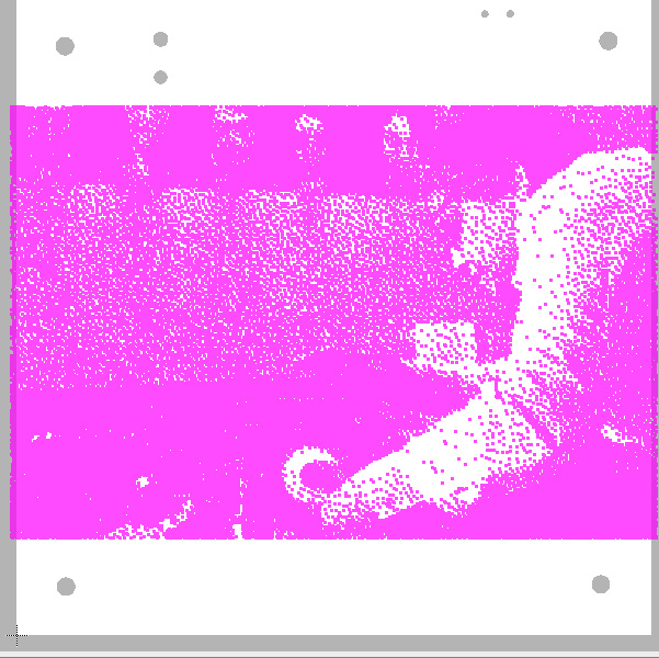
****
I also starting thinking that I should probably look at more existing DIY and pro analog video synth circuits…
A collection of great video synthesizer schematics resources : https://scanlines.xyz/t/diy-resources-file-system/224
Here are some of the ICs (that are still being manufactured) that I haven’t work with before that appear in several designs :
- Resettable and retriggerable Monostable Multivibrators : https://assets.nexperia.com/documents/data-sheet/74HC4538.pdf
- High speed diff comparators : https://www.ti.com/lit/ds/snosbj5c/snosbj5c.pdf?HQS=dis-mous-null-mousermode-dsf-pf-null-wwe&ts=1676232730602&ref_url=https%253A%252F%252Fwww.mouser.fr%252F
- Video Fader IC: https://www.analog.com/media/en/technical-documentation/data-sheets/12516fa.pdf
- Graphic EQ display filter : https://www.sparkfun.com/products/10468
To divide a signal into 8 different bands (if you skip the MUX at the end) :
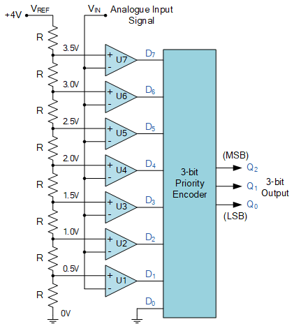
Here’s a simple implementation with a 4051 analog mux at the end :
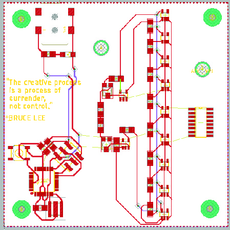
This worked after I sorted out that the Atmega 328 reset was pulled LOW all the time – so it programmed fine but never did anything after that. I also removed the op amps which were supposed to follow the selected thresholds, I connected the top and bottom directly to the pots in the end. I tried slowly switching between bands at half a second and also faster at 50ms. Both as expected.
And I’m revisiting all kinds of combined capacitor + switch circuits which move tiny charges around based on signals :
- sample and hold
- bucket brigade
- comb filter
- switched capacitor circuit
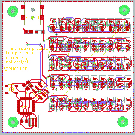
I have made this bucket brigade “delay” with 50 microchip tunable (variable) 100-200pF capacitors :
I am now curious about some other capacitor switching circuits like this Comb Filter : https://en.wikipedia.org/wiki/Comb_filter which somehow “provides response” at different multiples of 1KHz depending on 3 bit code. All the caps are the same value.
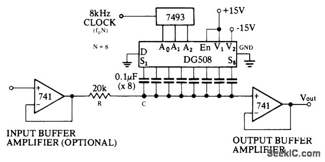
Here is another circuit design for the same function :

****
For the FPGA board, I’ve ordered an iCE40HX1K development board and am currently planning to test some basic VGA signal generation. The next steps could involve basing a design off of the OLIMEX dev board design (https://github.com/OLIMEX/iCE40HX1K-EVB/blob/master/ICE40-1KEVB_Rev_A.pdf) which already has SRAM and VGA OUT along with code on the internet (which I would follow closely for the first iteration). I would alter the board to be able to program directly via USB using the components from the Ice40 stick ( https://www.mouser.fr/new/lattice-semiconductor/lattice-icestick-kit/), like a fancy new FTDI chip, so I could stay within the Lattice software for my first steps.
Compared to the VGAX, the FPGA could generate signals much faster (being clocked with a 100MHz crystal versus the 16MHz of the Atmega), it would also be producing signals based on a a different coding paradigm (I have no idea what that would mean in terms of images), and because it has around 90 I/O it could also work with super deep colors using only a R2R ladder. The possibility of using an SDRAM is so cool but it seems hard to implement, with SRAM being much simpler to interface. The OLIMEX has only 512KB of SRAM, so I couldn’t really record a lot with it.
****
Here is my process for the FPGA programming so far :
- I signed up for an account at www.latticesemi.com.
- I got a licence for iCEcube2, put it somewhere easy to find and took note of the directory, and downloaded iCEcube2 and the Lattice Diamond software from here : https://www.latticesemi.com/en/Products/DesignSoftwareAndIP
- I plugged in the iCEstick and it blinked in a circular pattern. I also checked that it had a port under Device Manager (it had 2!).
- I went into iCEcube2 then to Help > Tutorial to open a pdf called “Implementing the Design” and followed the following steps :
- Start new project (iCE40, HX1K, ?TQ144?)
- Add Design file iCElab.v and Constraint file iCElab.sdc and checked the Device Info.
- Run Synplify Pro Synthesis
- Select Implementation
- Add constraint file iCElab.pcf under Import P&R Input Files.
- Run Placer
- Check the Floorplan, package view, timing analysis, power estimation
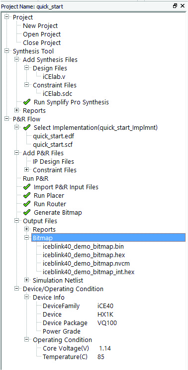
- Generate the bitmap (.bit and .hex files) which is saved wherever the project was saved. (For instance C:\Users\Jonah\Desktop\FPGA LATTICE DEMO PROJECTS\quick_start\quick_start\quick_start_Implmnt\sbt\outputs\bitmap).
- Here is what everything should look like once finished :
- I then transitioned to Youtube for a detailed explaination of using Diamond Programmer with the iCEstick here : https://www.youtube.com/watch?v=Df9k1T0bHmA&ab_channel=Dom
- Launch Diamond Programmer and take the default options (or click scan and take those)
- It will mistake the board for a JTAG interface and give the following errors : “Failed to scan board”, “Scan Failed – Creating Blank Programmer Project.”
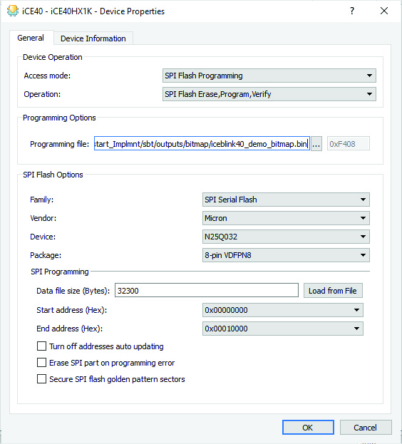
- Now change the Device Family to iCE40, the device to iCE40HX1K, and under Program enter the following information :
- Change Access mode to SPI Flash Programming and now some other options appear. Select > Vendor: Micron, Device: N25Q032, Package: 8-pin VDFPN8
- Now load the bitmap (.bin) file and check that it has a non-zero datasize :
- Click OK and then click the green traffic light on the next to top row of icons. You should then see a completion message and have the program on your board :
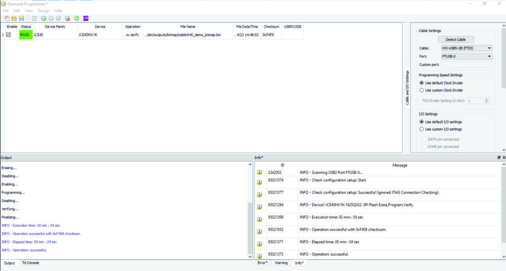
- Presto !
Just for info :
For the actual pinout of the ice40 (which you can change in Pin Constraints Editor):
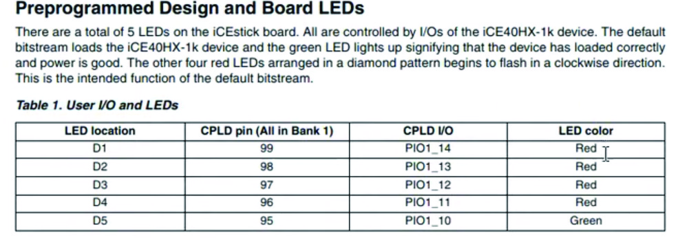
Generating your own .v file, you can open Notepad++ and paste :
module AND( input A, input B, output Y ); assign Y = A&B; endmodule***
Here’s what ended up getting presented :

Here is the text I made to go with it :
My takeaways :
Do something simple, and humble, but try to do it well. Trying to do too many things, or a “universal” thing, or a multi-functional reprogrammable thing is really ambitious. This has happened to me before :
- At the Barilla Hackathon (the team that did the best made a simple lunch surface, it was simple but really well made and designed).
- With my solar robot project (the one that was supposed to run on solar energy and no battery, interact with other robots, and possibly build a structure)
- With my original solar sunflower design that was supposed to look super intricate.
Making a machine that works for a demo is the highest level of challenge. It requires you to master the functining of the machine to a high degree to be able to fix it and adapt in changing conditions. It you do something simple, you have a higher chance of being able to do this.
It would have been important to realize that the place this was to be shown is a corporate environment, and that my interest in the bodge / bricolage would never have found its place here. The corporate mentality is shiny, new, pro-tech, and “impressive”. I should have understood this before taking the project.
The simple, distilled, purified, humble and clear idea from this project was the wooden-mounted electronic circuits. This would have been in line with my “design research” interests, my aesthetic.
If I were to make a complex machine like the one I had in mind for this expo that would have worked, I think I would have to change the following things :
- Generate my own VGA signals. For plug and play things, generating this in software seems so much easier because you are the one making it and you have control over what is being produced.
- Figure out, once and for all, the story around shared grounds and blocking caps, and bias pots, and voltage in and voltage out levels, for different modules. Also, 75ohm resistors and small caps before VGA out ? Should I just get a VGA driver chip that works? (EDIT: Here is an explaination of how to calculate the output impedence for VGA cables : https://hackaday.io/project/18682-pic-graphics-demo/log/49786-vga-interface)
- I would need to figure out what makes the VGA monitor turn off (is it sending something it doesn’t consider a video, or a voltage level that is too high?)
I think the alternative, which would be showing pre-recorded videos, is uninteresting for a performance. Another key ingredient I think is having designers / artists to help me review the project regularly (like in design school). It should also be really clear to me if it is my design project or a commission (in which case I’m an engineer I guess?). I should also get clear right from the begining next time what are the conditions of the final thing – where will it be, what are the goals of the person commissioning the work, etc.). I should probably only work with people who share my interests and aesthetic !
I think I have to acknowledge that I have an extremely constrained working process that is highly method driven. I am not focused so much on the end product directly. My friend suggested I was over constraining myself. Basically there is a confusion between whether I’m using technology to stumble upon unexpected things, or whether I’m using it to make something that works. To work efficiently on things would work well would require time developing the things that must work well, and an organized, systematic working practice. I MUST ORGANIZE MY ELECTRONIC PARTS to make this process more efficient.
Also : all the intense pressure and hardcore work streaks I put in DID NOT HELP THE FINAL PROJECT – I can’t even think straight or debug basic circuits right now :(. It would have been better to perhaps start working on the final thing starting on day 1, with the EASIEST, SIMPLEST, AND MOST LIKELY TO WORK PAINLESSLY solutions.
Another key question is what is the output, and who is my audience ? I need a way of mesuring my output and comparing it.
- Am I making art for people who consume art ? (then I have to move towards very simple projects and focus on their EXECUTION while photographing everything super well for my PORTFOLIO)
- Am I making “design research” papers/talks for academics and people who consume this ? (then I need to WRITE about my research)
- Am I making open-sourced electronics kits for hobbyists ? (Then I need to spend time ENGINEERING working kits that people would be interested in making)
- Am I making workshops for designers ? (Then I need to come up with simple exercises for workshops?)
And am I doing several of these things simoultaneously ? I think doing any one of them well first could take a lifetime already ! My friend suggested projecting five years in the future to where I would like to be and building backwards from there. I think I would most like to be a teacher who does art/design research in the form of expos, articles and classes (a bit like Andrew Witt at the GSD).
********
Where I would like to go from here :
- Test my basic FPGA VGA board. What can it do with video ? Possibly make another pro version (USB programmale, nicely laid out, SRAM). FPGAs feel like the future because they are good a processing video in parallel, and because coding them is essentially like building 74 series logic circuits but without all the soldering. It could also lead to some cool machine learning experiments later on..
- Test my automatable SRAM 4MB board. What kind of automatic looping can it make?
- Try to get the SPI SRAM board functioning (it is so simple it would be perfect for a video sampling workshop). It would be cool to see what kinds of images it produces. It works at 20MHz, it would be perfect !
- Get Spaghettini working with aluminum board (just avoid going through-hole) – this is the simplest way to generate cool simple memory based video !
- Have another stab at presenting my work as an art installation at my show end of march at La Générale.
- Try the bucket brigade and digitally controlled pot boards
*******
After my colleague Fabien told me about EDID EEPROMs, I am thinking it could be possible to mess with the memory of this EEPROM that communicates with the computer sending VGA signals and create some interesting glitches this way : https://en.wikipedia.org/wiki/Extended_Display_Identification_Data
Also check out these types of RAM :
- https://en.wikipedia.org/wiki/Dual-ported_RAM
- https://en.wikipedia.org/wiki/GDDR_SDRAM
And this keeps coming up when looking into controlling screen rows and columns directly : https://en.wikipedia.org/wiki/Low-voltage_differential_signaling
Check out no input mixing and electro-acoustic musique concrete, and machine exorcism.
Check out universal LCD driver IC RTD2556 on boards like this :

***
It looks like I could build my own HMDI to VGA converter with two AD ICs : https://www.analog.com/en/analog-dialogue/articles/hdmi-made-easy.html
I could combine this with a new board that uses a bunch of SPI SRAM memory chips controlled by arduino to approximate the 7 channel 4MB recording and mixing board I made.
I could also put a rasbpi zero with just power, an SD card containing videos and an HDMI mini out. For the Raspberry Pi I made the HDMI hot pluggable (hdmi_force_hotplug=1) and put a bunch of low res mp4 videos in the boot SD card which are accessible.