Heading towards a more reliable, deployable and software-leaning approach (but not so much about automated choreography as with previous atmega boards as augmented live playable machine for manual performances) to working with video now.
I am also trying to be a bit more strategic and attempt to think ahead a little bit beyond the one board one experiment situation. It takes a long time to trouble shoot a single board and learn all the lessons from it, I have to give each board the time it deserves and I need to be perhaps less productive and more thorough.
I am also coming to the awareness of what is my scope with this next board :
- I won’t be doing challenging engineering things (like implementing different ways of programming the same FPGA, interfacing with differential pair protocols like HDMI) that have no impact on the images and take loads of time to do.
- These are boards for experimenting and live playing, so they also need to have controls on the board.
- I also need to think about safety, avoiding the possibility of easily making short circuits and damaging the board.
- I’d also like to move back to color, and away from the intense limits of exclusively 1bit resolution.
- I want to keep removing superfluous cables and adapters too, this one will have only a VGA out.
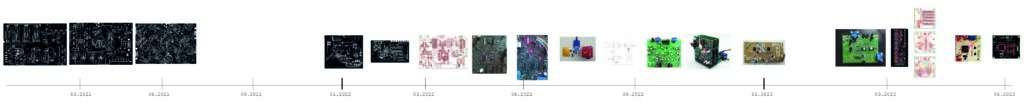
I made a map of my prototypes so far for this project :
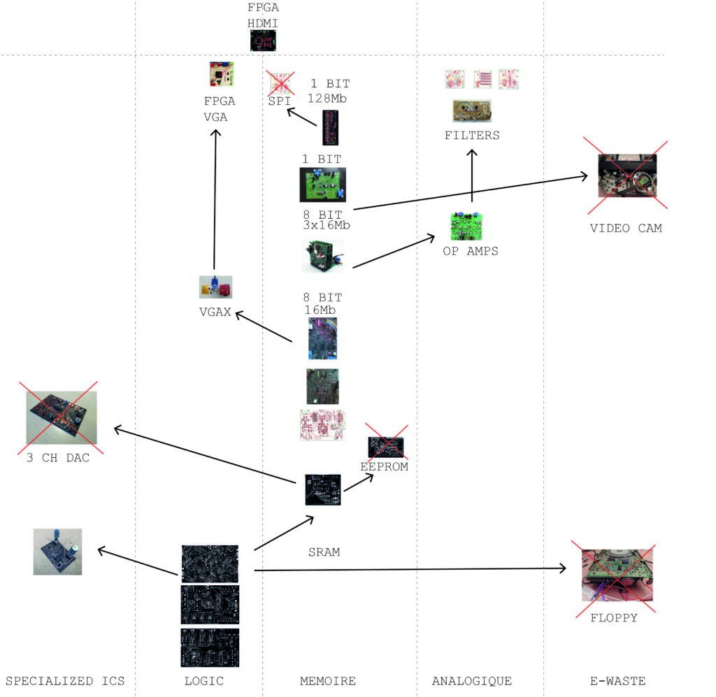
It’s been around two years I’ve been working on this !
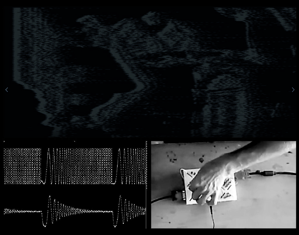
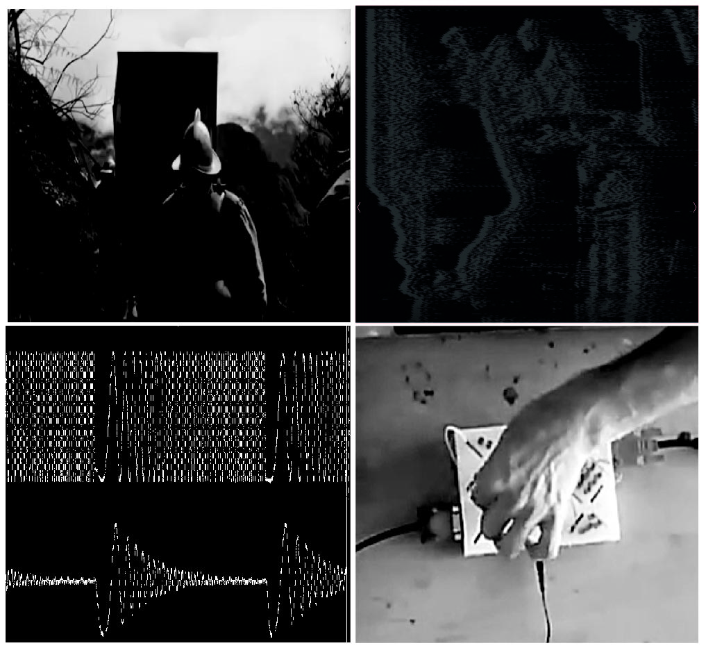
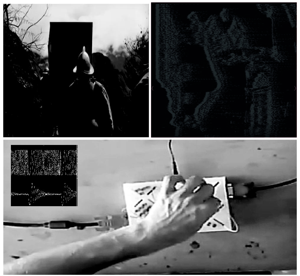
After talking with Zach at work, his idea was to show not just the screen but also me turning knobs etc. Here’s what this could look like :
Or,
…or,
It would be nice to have a computer interfaced oscilloscope to record the signals.
*****
The most plug and play option would appear to already exist : a tiny raspberry pi zero can already run Processing scripts and control small screens https://learn.adafruit.com/processing-on-the-raspberry-pi-and-pitft/processing !
Here’s a good intro to making simple patterns with processing : https://processing.org/examples/
We would be more in the zone of software video synth : https://learn.adafruit.com/feather-rp2040-dvi-video-synth
Also seem to be companies making just this kind of thing : https://store.excamera.com/
Arduino talks to the FPGA by SPI as if it were a RAM space. https://excamera.com/files/gameduino/synth/doc/gen/poster.pdf
Design / Engineer friend Paolo Salvagione pointed me to Configurable mixed-signal ICs. It appears to be like an FPGA but for mixed analog and digital circuitry and is configured in design software.
There is also the world of ASICs and the google open-source silicon project https://developers.google.com/silicon
*************
My project was originally about slowing down computer processes and representing them in space. Now I just seem to order things on Amazon and design increasing numbers of PCBs. It seems that I have so little time to do the art in the end because of how much investment the technical stuff requires. How could I get back to my original project here ?
My project also had a collection of related techniques :
- Try to free machines from their corseted, factory settings and reveal their full range of expression that would otherwise just exist in a parallel unseen dimension
- Try to show our files from the perspective of / through the eyes of the machines that are processing them.
- Curate series of abstract formal compositions which emerge from figurative, architecturally-themed or culturally iconic ones.
- Try to describe the behaviour / idiosyncracies of algorithms and make them tangible
- Isolate specific moments of machine-to-machine interface in a larger system
- Get one’s hands inside the black box, and make prepared machines which expose their parameters
- Try to rebuild electronic systems based on help from the DIY internet and then hope to stumble on something unintentional
- All the while emphasize the materiality of technology
- Trying to go super low-level and avoiding abstract computer “visualizations”
- Exploring the link between visual chaos and harmony, that sweet spot of medium entropy.
- Riffing off of the music synthesizer movement of knobs and playful electronics interfaces and its anti-theory vibe
- Exploring the surreal, bizarre space of the computational unconscious
- Do “artistic research” projects that are educational, at least for me
- play with form versus content
I wonder if the pixel based screen is not really appropriate for my methodology. It’s the opposite of over-looked and black boxed. It’s an obsession for an entire culture. It also does a pretty good job of “representing” what happens inside the computer already. It doesn’t really need my help !
********
I also need to do a debrief on this leg of the video synth project. What have I learned ?
Technical stuff :
-
-
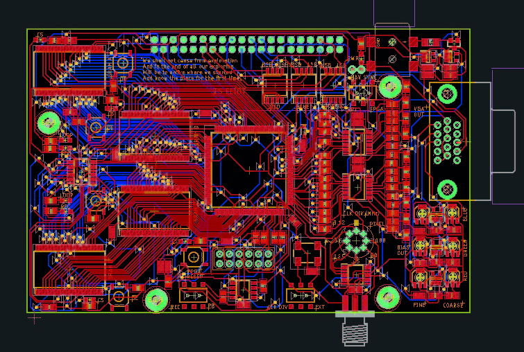
- How to make and debug PCBs
- To work with video + SRAM with counters as well as some op amp circuits. The difference between digital and analog in the video context.
- To work with the VGA protocols, about resolution and brightness of the image.
- I learned about oscillation, the difference between KHz and MHz in the context of video and what sampling is.
-
Stuff about media representation
-
-
- some aspects of the nature of visual memory, how some of our sensory apparatus work at different speeds
- the curious experience of “searching” for an image (like when messing with ADC knobs and CLK speeds).
- what is required to identify / recognize and image or scene, how much resolution and shape
- Deconstructing the illusion of television by interacting with its materiality and mutability
- Repeating historical art explorations with television (see Sans Soleil – Chris Marker)
- synchronizing the data with the frame of the image is a key part of the illusion of video. If you mess with this suddenly the video frame becomes a malleable object. If it is desynchronized, the image is out of frame and will jump around with the SRAM recording. If you change the speed of recording or of playback you can zoom.
- Layering of different images in a palimpsest can create textures from them.
- I’ve made some nice abstract pattern discoveries through knob twisting.
- Exploring the gap between legible figurative image and abstract patterns, contours, fields,
- the texture and grain of data at various scales
- the connection between video and abstract field painting
-
What does it mean to be trying to make super simple hardware video filter in the age of AI generated video and images ? How is this activity relevant ? I feel like I’m looking for low hanging fruit here but I’m not sure there is any left. Also, the time it takes to make a single experiment in hardware is astronomical compared to the software option…
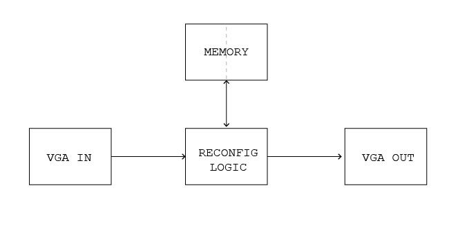
I think the project started off about the screen itself, how to send signals and display them. At some point it became clear that the screen just displays data stored in memory.
In this spirit, I could try to represent memory access patterns : https://en.wikipedia.org/wiki/Memory_access_pattern Or the patterns that memory is refreshed in : https://en.wikipedia.org/wiki/Memory_refresh
http://www.overbyte.com.au/misc/Lesson3/CacheFun.html
I could also sample images and then modify them algorithmically? But it kind of ends up looking like simple Photoshop filters. It would have to be modified in some way based on the way the image is stored in the memory ?
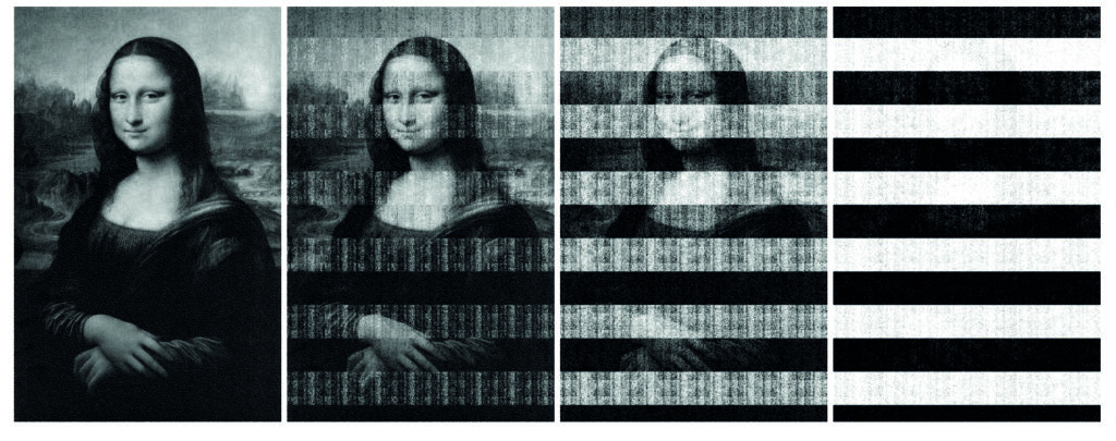
Check out this image stored in DDR ram decaying over time from J. Alex Halderman’s paper : https://jhalderm.com/pub/papers/coldboot-sec08.pdf
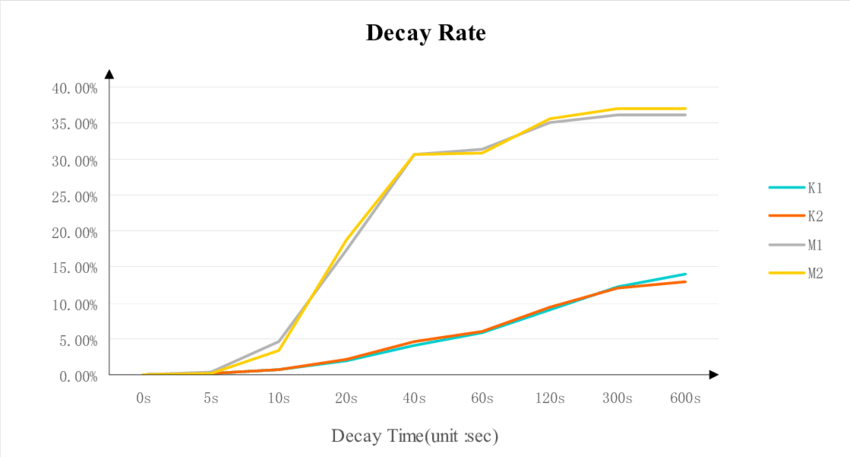
Also it seems like different DDR has different decay rates (from A Trustworthy Key Generation Prototype Based on DDR3 PUF for Wireless Sensor Networks https://www.researchgate.net/figure/DRAM-cells-decay-feature-with-power-switch-interval-time-of-120-s-a-DDR3-device-1-b_fig3_263586301):
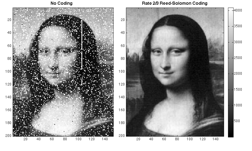
For comparison, check out the same Mona Lisa image sent through the air and damaged by the earth’s atmosphere :
********
I’ve never thought of this before but I guess I could generate a simple arduino code, and then take the .hex file and glitch it with any of the glitching techniques I’ve been using and see what it puts on screen.
I could also test overclocking / overheating the atmel and seeing how they collapse !!
********
I should also finish the boards I’ve already designed and had made, they offer learning opportunities and possible discoveries ! The bucket brigade, the digitally-controlled pots (meh), and the band splitter (*EDIT* completed !) are the three that are left from that series. Also the Palimpsest.OS 2 board when controlled by microchip – especially if I can get the sync working ! Of course I have the new 128Kbit memory board (*EDIT* all done !) once I get the parts too and then a final (?) FPGA v2 board.
********
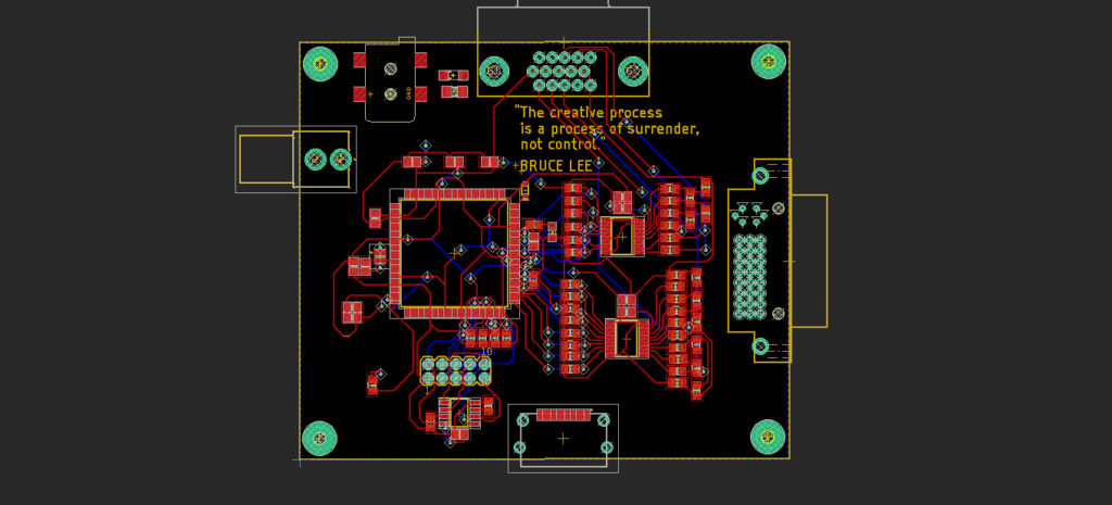
I am still interested in exploring FPGAs and getting my hands in the tech to possibly stumble on cool stuff though so here is a second attempt at a video FPGA board based on the iCE40HX1K-TQ144 to output HDMI, DVI, VGA, and composite video.
For generating verilog, there is migen for python 3 (https://github.com/m-labs/migen). I’m going to try a super simple thing in Verilog first to get a feeling for it.
I am learning verilog here : https://hdlbits.01xz.net/wiki/Main_Page
It looks like generating HDMI is doable even though there is a difference between LVDS and TMDS (involving possibly 100nF series capacitors ?) :
Here is the official guide : https://www.latticesemi.com/-/media/LatticeSemi/Documents/ApplicationNotes/UZ/FPGA-TN-02213-1-7-Using-Differential-IO-LVDS-Sub-LVDS-iCE40-LP-HX.ashx?document_id=47960
https://www.fpga4fun.com/HDMI.html
blackmesalabs.wordpress.com/2017/12/15/bml-hdmi-video-for-fpgas-over-pmod/
https://github.com/hdl-util/hdmi/
Different chips being used like the PTN3360D HDMI / DVI Level Shifter (IN STOCK!), a TFP410PAP TFP410 TI PanelBus™ Digital Transmitter (NO STOCK!),

According to the datasheet, “The LVDS25E/subLVDSE differential output buffers are available on all banks but the LVDS/subLVDS input buffers are only available on Bank 3 ofiCE40 LP/HXdevices.” ***Those are INPUTS but there are no special OUTPUT pins.***
I have replaced the LDO with was giving me trouble previously and am making this version USB programmable so it could be a useful for others as a cool video kit.
*****
Revisiting FPGA programming, here is where I got to last time :
Here is my process for the FPGA programming so far :
- I signed up for an account at www.latticesemi.com.
- I got a licence for iCEcube2, put it somewhere easy to find and took note of the directory, and downloaded iCEcube2 and the Lattice Diamond software from here : https://www.latticesemi.com/en/Products/DesignSoftwareAndIP
- I plugged in the iCEstick and it blinked in a circular pattern. I also checked that it had a port under Device Manager (it had 2!).
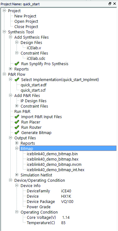
- I went into iCEcube2 then to Help > Tutorial to open a pdf called “Implementing the Design” and followed the following steps :
- Start new project (iCE40, HX1K, ?TQ144?)
- Add Design file iCElab.v and Constraint file iCElab.sdc and checked the Device Info.
- Run Synplify Pro Synthesis
- Select Implementation
- Add constraint file iCElab.pcf under Import P&R Input Files.
- Run Placer
- Check the Floorplan, package view, timing analysis, power estimation
- Generate the bitmap (.bit and .hex files) which is saved wherever the project was saved. (For instance C:\Users\Jonah\Desktop\FPGA LATTICE DEMO PROJECTS\quick_start\quick_start\quick_start_Implmnt\sbt\outputs\bitmap).
- Here is what everything should look like once finished :
- I then transitioned to Youtube for a detailed explaination of using Diamond Programmer with the iCEstick here : https://www.youtube.com/watch?v=Df9k1T0bHmA&ab_channel=Dom
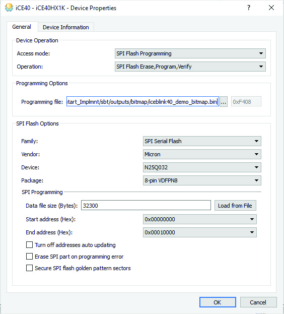
- Launch Diamond Programmer and take the default options (or click scan and take those). Important to note that you must launch Lattice Diamond Programmer directly, not through Lattice Diamond, in order to find the iCE40HX1K chip.
- It will mistake the board for a JTAG interface and give the following errors : “Failed to scan board”, “Scan Failed – Creating Blank Programmer Project.”
- Now change the Device Family to iCE40, the device to iCE40HX1K, and under Program enter the following information :
- Change Access mode to SPI Flash Programming and now some other options appear. Select > Vendor: Micron, Device: N25Q032, Package: 8-pin VDFPN8
- Now load the bitmap (.bin) file and check that it has a non-zero datasize :
- Click OK and then click the green traffic light on the next to top row of icons. You should then see a completion message and have the program on your board :
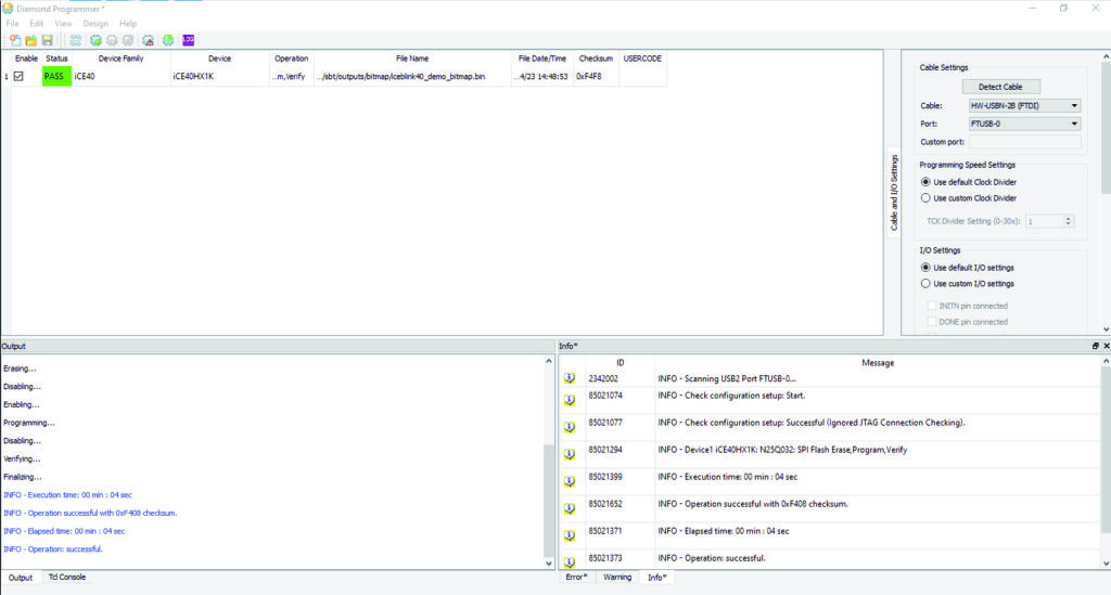
- Presto !
Just for info :
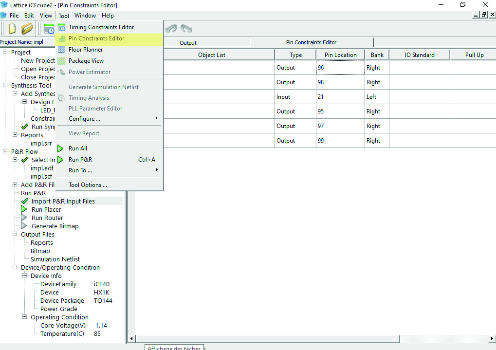
For the actual pinout of the ice40 (which you can change in Pin Constraints Editor):
***
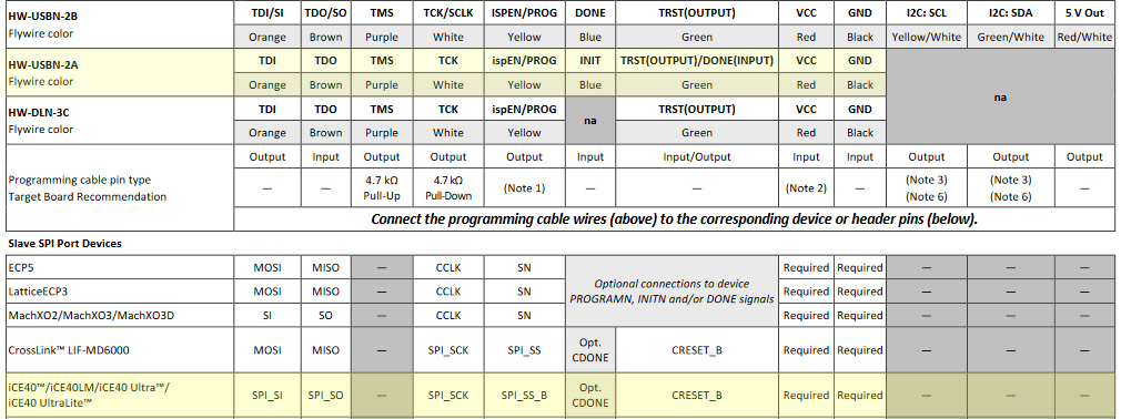
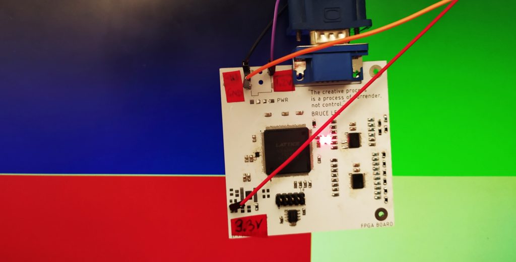
And here is my attempt programming my own board with the Lattice Programmer.
I followed the same steps as above but instead selected the HW-USBN-2B (FTDI) programmer. Important to note that you must launch Lattice Diamond Programmer directly, not through Lattice Diamond, in order to find the iCE40HX1K chip. Also note that you need Lattice iCEcube2™ Software, not just Diamond for some reason.
Here are the color connections needed from the Lattice Programming Cables User Guide :
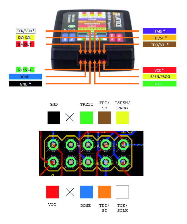
The USB power and Board power lights should be on on the programmer and the Prog blue LED should flash a few times before the Done blue LED will flash and Lattice Programmer will display Operation: successful.
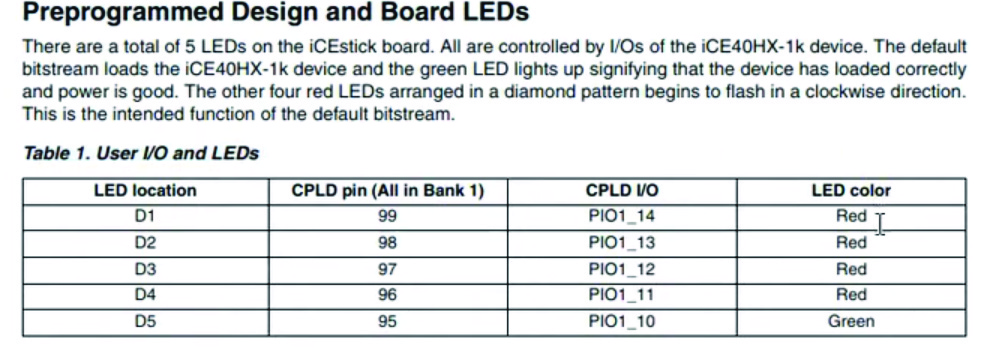
I am taking the example LED rotation verilog .v code :
module LED_Rotation(

    input  clk,
    output LED1,
    output LED2,
    output LED3,
    output LED4,
    output LED5

    );

               reg[15:0] div_cntr1;
               reg[6:0] div_cntr2;
               reg[1:0] dec_cntr;
               reg half_sec_pulse;

               always@(posedge clk)
                              begin
                              div_cntr1 <= div_cntr1 + 1;
                              if (div_cntr1 == 0)
                                            if (div_cntr2 == 91)

                                                           begin
                                                           div_cntr2 <= 0;
                                                           half_sec_pulse <= 1;
                                                           end
                                            else
                                                           div_cntr2 <= div_cntr2 + 1;
                              else
                                            half_sec_pulse <= 0;

                              if (half_sec_pulse == 1)
                                            dec_cntr <= dec_cntr + 1;
                              end
               assign LED1 = (dec_cntr == 0) ;
               assign LED2 = (dec_cntr == 1) ;
               assign LED3 = (dec_cntr == 2) ;
               assign LED4 = (dec_cntr == 3) ;
               assign LED5 = 1'b1;

endmodule
Under Tool > Pin Constraints Editor, we can change the pins activated in the code but mine is already set up connected to pin 99:
I am soldering a second FPGA board. I noticed that the clock was not outputing anything, and also that the max temperature for the IC for reflow soldering is around 250°C. I am making sure to use the soldering iron “kissing” technique along with loads of flux applied.
Reading through the datasheet :
- Bank 3 additionally supports differential LVDS25 input buffers.
- Each bank can have it’s own voltage level.
- I may have to power the VCC, VCCIO_2, VCC_SPI, VCC_PLL, and VPP_2V5 (with a diode) even if I don’t plan on using them all just to get the device to turn on. (There is even a proper sequence to power them up in).
- GNDPLL must NOT be connected to the board’s ground !
- Bank 2 has two dedicated Input pins.
****
FPGA BOARD ERRATA / DIARY :
- 1.2V is connected to 5V throughout because of an EAGLE issue 🙁
- I tried the voltage regulator 3 times and still no luck. *UPDATE* I tried a second 1.2V LDO that I ordered and it still reads 2.2V or so. No idea why this is happening when I can power the pin directly with 1.2V with my power supply no problem (therefore it can’t be a bad connection somewhere between 1.2V and another trace right?). Positive news is that the FPGA appears to have survived the over-voltage !!
- Maybe I should give it a higher frequency oscillator, at least 25MHz, as I’m working with video?
- I connected pin 9 of VGA to GND, it is connected to 5V on the signal side !
- The GNDPLL should not be connected to GND.
- The R2R ladder has a 270ohm going to ground instead of a 536 on each ladder.
- Unclear which pins to plug where for programming – *EDIT* SOLVED
- I had a hard time at first soldering the FPGA but then discovered a soldering “kiss” technique that was reliable and effective. For the clock, I melted the solder and then placed it gently on top.
- I plugged it in with 2.2V instead of 1.2V and likely destroyed the chip the first time…
- 0805 is doable and better for compact designs
- I can’t find the name of the chip in the Target Device menu of Diamond Programmer. *EDIT* SOLVED : You need to open Diamond Programmer directly.
- I need to get nicer boards if I am going to be working on FPGA boards, Aisler not inexpensively manufactured.
- It seems like exploiting the parallelism of the FPGA could be interesting to explore. For this project it would probably be to logically mix several input videos together while transforming ?
***
I’ve got it blinking at different frequencies !
Now I want to generate some VGA signals as quickly as possible and start creating images by tweaking pre-made code like for VGAX.
And here is demo code for the OLIMEX ice40 developement board which has RAM, DAC, ADC and VGA (but it needs a 100MHz clock) : https://github.com/OLIMEX/iCE40HX1K-EVB/tree/master/demo/ice40-io-video
Also super simple (but uses a 25MHz clock) : https://www.fpga4fun.com/PongGame.html
Here is the one I ended up using (takes a 12MHz clock and turns it into a 25MHz with the PLL) : https://github.com/imuguruza/alhambra_II_test/blob/master/vga/vga_test/
Here is the key part of the code that actually draws on screen :
module vga_sync_test(
    input wire clk_in,
    input wire reset,
    output reg r0,
    output reg r1,
    output reg r2,
    output reg b0,
    output reg b1,
    output reg b2,
    output reg g0,
    output reg g1,
    output reg g2,
    output wire h_sync,
    output wire v_sync,
    output wire led,
    output wire locked_led
  );

wire clk_sys;
wire display_en;
//reg [9:0] h_count;
wire [9:0] h_count;
//reg [9:0] v_count;
wire [9:0] v_count;
assign  led = clk_sys;

localparam  h_pixel_max = 640;
localparam  v_pixel_max = 480;
localparam  h_pixel_half = 320;
localparam  v_pixel_half = 240;

//Check if we can create RGB colors
always @(posedge clk_sys) begin
  if (display_en) begin
    if (h_count < h_pixel_half
        && v_count < v_pixel_half) begin
      //Assign here your test color
      r0 <= 1'b0;
      r1 <= 1'b0;
      r2 <= 1'b0;
      g0 <= 1'b0;
      g1 <= 1'b0;
      g2 <= 1'b0;
      b0 <= 1'b1;
      b1 <= 1'b1;
      b2 <= 1'b1;
    end else if (h_count > h_pixel_half
            && v_count < v_pixel_half) begin
      //Assign here your test color
      r0 <= 1'b0;
      r1 <= 1'b0;
      r2 <= 1'b0;
      g0 <= 1'b1;
      g1 <= 1'b1;
      g2 <= 1'b1;
      b0 <= 1'b0;
      b1 <= 1'b0;
      b2 <= 1'b0;
     end else if (h_count < h_pixel_half
            && v_count > v_pixel_half) begin
      //Assign here your test color
      r0 <= 1'b1;
      r1 <= 1'b1;
      r2 <= 1'b1;
      g0 <= 1'b0;
      g1 <= 1'b0;
      g2 <= 1'b0;
      b0 <= 1'b0;
      b1 <= 1'b0;
      b2 <= 1'b0;
    end else begin
      //Assign here your test color
      r0 <= 1'b1;
      r1 <= 1'b1;
      r2 <= 1'b1;
      g0 <= 1'b1;
      g1 <= 1'b1;
      g2 <= 1'b1;
      b0 <= 1'b1;
      b1 <= 1'b1;
      b2 <= 1'b1;
      end
  end else begin
    r0 <= 1'b0;
    r1 <= 1'b0;
    r2 <= 1'b0;
    g0 <= 1'b0;
    g1 <= 1'b0;
    g2 <= 1'b0;
    b0 <= 1'b0;
    b1 <= 1'b0;
    b2 <= 1'b0;
  end
end

vga_sync vga_s(
      .clk_in(clk_in),         //12MHz clock input
      .reset(reset),           // RST assigned to SW1
      .h_sync(h_sync),
      .v_sync(v_sync),
      .clk_sys(clk_sys),       //25.125 MHz clock generated by PLL
      .h_count(h_count),
      .v_count(v_count),
      .display_en(display_en), // '1' => pixel region
      .locked(locked_led)      // PLL signal, '1' => OK
      );

endmodule
I would like to modify this code in the spirit of VGAX bytebeat-inspired video synthesis.
I made sure to load the three dependent .v files and then changed the pin constraints in the .pcf as follows :
set_io b0 76
set_io clk_in 21
set_io led 99
set_io r0 81
set_io b1 75
set_io g2 91
set_io r1 80
set_io v_sync 87
set_io b2 74
set_io g1 95
set_io locked_led 142
set_io r2 79
set_io reset 2
set_io g0 96
set_io h_sync 88
It works !
Just waiting for the LDOs to make it more practical to plug in. I will now test some actual patterns !
***
Here is my first test bench with ModelSim ! Thanks to this tutorial from Nandland : https://nandland.com/tutorial-your-fpga-program-an-led-blinker-part-2/
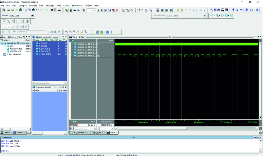
I am using ModelSim Lattice FPGA 2020.3 (which downloaded with either Icecube2 or Lattice Programmer?) and followed this PDF called
Using Mentor ModelSim Simulator with Lattice iCEcube2 (https://www.latticesemi.com/-/media/LatticeSemi/Documents/ApplicationNotes/MP2/Modelsim_AN006_Dec2020.ashx?document_id=50795)
The steps to follow :
- Open a new project
- Click Add Existing Files (pick only the test bench verilog file) and then Close
- Now Compilation > Compile All
- Now Simulation > Start Simulation
- In the console type <<view wave>>…
- …then <<add wave * >>…
- …and a time period for example : <<run 100ms>>. (It takes us, ns, ms, and sec it appears)
The signals are a little small and it is apparently possible to change this under Tools -> Edit Preferences, Wave Font and Footer Font…but when I try it crashes !
Looks like printing to the console is going to be useful ! They work by using display like so…
$display("0.5 seconds");…and then in the console area of ModelSim:
run -allHere’s a simpler version of a tb for a 10 ps period of the following module :
module dut ( input clk ); `timescale 1ps / 1ps
module top_module ( output reg clk );
dut instance2 (.clk(clk));
initial begin
clk = 1'b0;
forever #5 clk = ~clk;
end
endmodule***
Thinking about different ways of generating patterns on a screen :
- Screen coordinate based (plotting functions that take an input x and produce an output y)
- Time based + screen coordinate based (a counter t increases over time and modifies the function’s behaviour)
Turns out FPGAs can’t do math like microprocessors ! To implement trig functions you need to build a CORDIC, which is like a computer to calculate functions.
Then again there are some things FPGAs can do better than microcontrollers like cellular automata (one study I checked out said 36 times faster than a GPU and up to 2,800 times faster than software). HDL Bits has an exercise to build the rule 30, 90, rule 101, rule 184 cellular automata.
(Similar to cellular automata, it’s possible to make a hardware psuedo random number generator using a linear feedback shift register : https://en.wikipedia.org/wiki/Linear-feedback_shift_register )
Here was the solution to the rule 90 challenge that I had to look up in the end :
module top_module(
input clk,
input load,
input [511:0] data,
output reg [511:0] q);

always @(posedge clk) begin
       if (load)
           q <= data; // Load the DFFs with a value.
       else begin
          // At each clock, the DFF storing each bit position becomes the XOR of its left neighbour
          // and its right neighbour. Since the operation is the same for every
          // bit position, it can be written as a single operation on vectors.
          // The shifts are accomplished using part select and concatenation operators.

         // left                     right
         // neighbour              neighbour
           q <= q[511:1] ^ {q[510:0], 1'b0} ;
        end
    end
endmodule
Check out this processing sketch that is evocative of cellular automata :
https://openprocessing.org/sketch/1879926 or sketch 1908904
Could it be possible to do this live to recorded video with the FPGA and be able to vary the number of generations, speed, etc. ?
Try changing the “rules” live (by clicking “random”) while this cellular automata scrolls : https://devinacker.github.io/celldemo/
https://en.wikipedia.org/wiki/Cyclic_cellular_automaton
Makes one think that you could make a video game entirely from these patterns being activated at different times and in different zones…Or a dedicated FPGA board that takes in audio and divides it into different bands, or other control signals directly, to control which rules are being used to generate the pattern + a bunch of knobs to change the speeds etc. It could be super minimal, just some knobs, an FPGA and an HDMI out.
Hardware version of CA : tinkerings.org/2016/09/24/cellular-automata-explorer/
Also check out rules that go beyond logic operations with neighboring cells and into modulo values : https://en.wikipedia.org/wiki/Cyclic_cellular_automaton
I am now trying to use the test bench to better understand why this code isn’t putting any pixels on the screen currently.
Here is my test bench. An important note is that variables that are not modified in an always or initial block should not be reg but wire instead.
`include "rule90.v"
`timescale 1ps / 1ps


module rule90_tb();
reg clk;
reg load;
reg [511:0] data;
wire [511:0] q;

rule90 DUT (
.clk(clk),
.load(load),
.data(data),
.q(q)
);

initial begin
#10
clk = 1'b1;
#10;
clk = 1'b0;
#10;
load = 1'b1;
data = 1'b1;
clk = 1'b1;
#10;
clk = 1'b0;
#10;
load = 1'b0;

end

always #10 clk = ~clk;
endmodule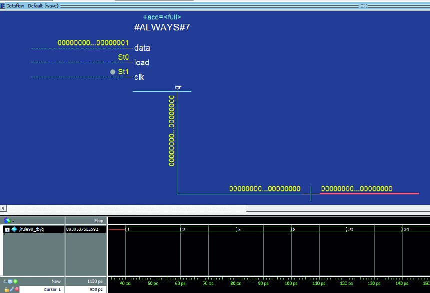
This shows that the rule90 circuit is working. Every clock cycle it advances. If I could show one bit per pixel and refresh every clock cycle ?
***
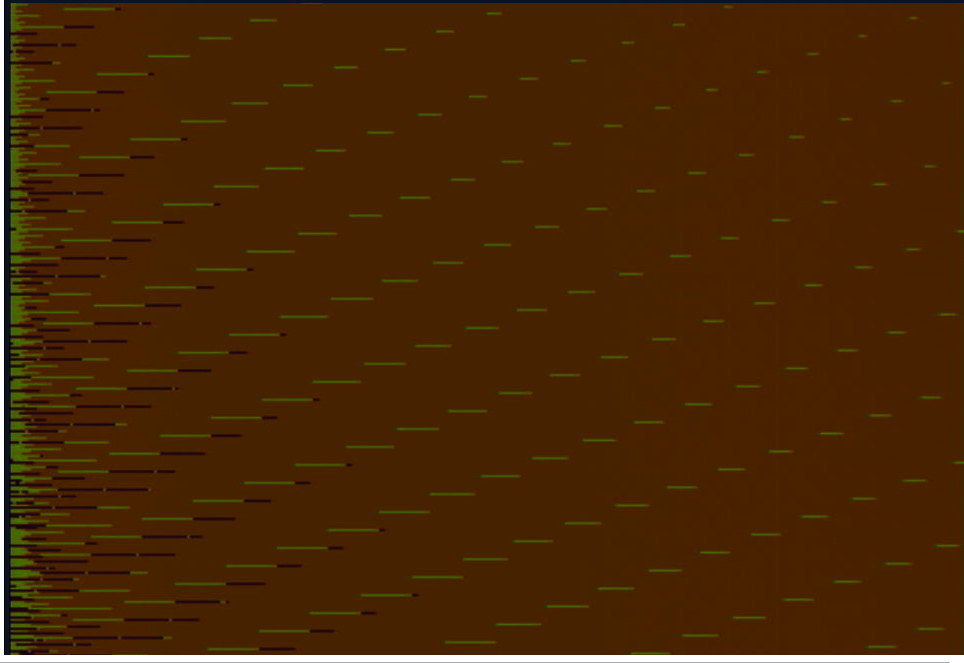
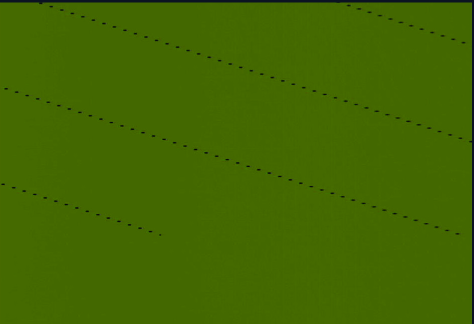
I’m getting some cool images :


***
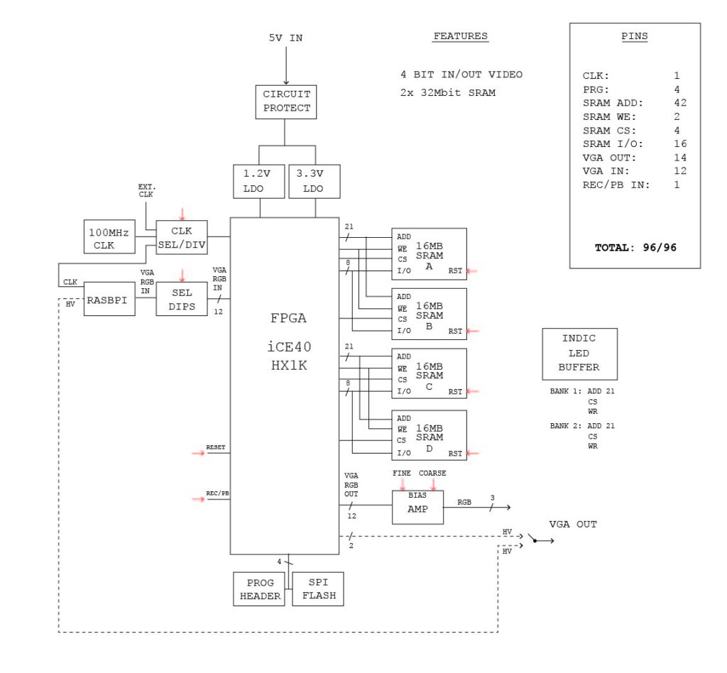
For the next FPGA board, I’m aiming for the following features :
It could have a handy mini screen (raspberry pi zero using DPI I/0 pins with video splitter to pass on the VGA to FPGA).I wonder if this isn’t a gimmick and not really in line with the “artistic research” aspect of my project.FTDI chip for USB programming(this is too technical I have decided)- 100MHz oscillator with divider
- 4x SRAM, possibly in two banks as I only have a total of 95 pins to work with
HDMI out, (possibly composite and DVI also ?).I wonder if this isn’t a gimmick and not really in line with the “artistic research” aspect of my project.- Some kind of basic interface ? (Knobs etc? But this would require an ADC unless I just use dip switches). One solution is to make hardware controls on the peripherals (clock divider, bit selections for incoming and outgoing signals, reset and CS sel on SRAM, etc.).
An atmega which can ask the FPGA to do things?Not sure this is necessary.A fan and heat sink for the FPGA??But this will hide it. Also a gimmick.An FPGA with more Logic Modules – like 4K instead of 1K?But this doesn’t come in the easier to solder format…- A reset button ?
- A fuse and reverse polarity protection !
microcontroller-accessed SPI FLASH so we can test moving between different types of memory.Except I haven’t had a lot of luck with SPI memory and video recording so far.
Reading a bit more about what FPGAs can do well ;
- they have tons more I/O pins than an Arduino? This means I can control multiple SRAM address and I/0 pins.
- Architecture can be completely reconfigurable (unlike a microcontroller which keeps the same architecture).
- low latency applications that take data as a stream in real time from sensors, cameras, etc. This means I can perform fast logic manipulations of saved data.
- high throughput applications, pipelining
- encryption and networking
- digital signal processing (IIR, FIR, FFT, ADC, DAC) like video filtering
- parallelism, like doing 128 small tasks at the same time, versus microcontrollers doing things in serial
- algorithms that can be solved with LUTs, tasks with lots of small adding and subtracting or multiplication (?)
- K-means clustering, Monte Carlo, neural nets, Mandelbrot fractals, cellular automata ?
- Seems that there are more and more systems that include micrcontrollers + FPGA + DSP, and you can of course put a microchip inside an FPGA. Here the FPGA accelerates certain tasks for the CPU
*****
Here’s what I think I could do with an FPGA and two individually-accessible SRAM I/0 banks banks :
- Reverse, scramble, or move through memory addressing with different patterns
- could change the sample rate of recorded or incoming images
- could perform logic operations on incoming /recorded video
- could place sprites on screen, or other parts of memory, through blitting I could selectively overwrite memory.
- It could record 8 tracks in parallel at 1 bit resolution, or record super long 1 bit resolution videos like on previous boards.
- It could do matrix transformations on memory like shear, rotation
- Copying values from one address and then reapplying them to another address every frame (called piping) or just one time. I could generate noise between certain values, or shift values up or down on (called tilting), listen to a value and then reapply it after a fixed number of frames, freezing the current value somewhere for future frames, replacing values intelligently with values in certain sets. Could this be called in-memory processing (https://en.wikipedia.org/wiki/In-memory_processing)? I could copy all the kinds of ways memory is accessed : https://en.wikipedia.org/wiki/Memory_access_pattern !

With this setup, the FPGA can increment the ADD of all memories while individually controlling which SRAM is reading or writing. Additionally, and simultaneously, it can send and receive different data between two connected SRAM banks. Bascially, it can’t simultaneously access two different parts of memory for reading or writing, if it wanted to do that it would need to remember some info in a buffer and then change the address in sequence like a normal microchip (this is all to give a greater color range to the board). So as far as I can tell the following memory reading and writing operations could be accomplished :
- while incrementing memory ADD, record incoming video on A, B, C, D in sequence (at various bit depths)
- while incrementing memory ADD, record incoming video on A, B, C, D in parallel (make 4 copies)
- while incrementing memory ADD, record incoming video on A, B, C, D and playback previously recorded video
- while incrementing memory ADD, play back video on A, B, C, D in sequence
- while incrementing memory ADD, playback video 4 copies of a video on A, B, C, D in sequence (i.e. loop)
- while decrementing memory ADD, playback a video in reverse
- access recorded video with different ADD patterns
- while incrementing memory ADD, take stored sprites from the top of one SRAM and insert them into over SRAMs at later addresses
- while incrementing memory ADD, perform logic operation on incoming video + an SRAM reading while writing it to a second SRAM
- while incrementing memory ADD, perform bit level transformation on an SRAM recording while writing it to a second SRAM
I am starting to think that losing some color information is worth having more flexibility to work in parallel with SRAM and save me headaches later on when I’m doing verilog hardware descriptions. Here is a simpler proposal that would have a single input (possibly record/pb or “function” meaning do something to the incoming video and then show it on a loop) :
- I lose LEDs, but I replace them with the most honest indicators possible, the signals themselves buffered.
- Lost the ability to control individually each quarter memory with WE control.
- No more DIP select buttons…How will I be able to play this thing live once it’s going through its code (apart from being able to mess with the clock, the RGB bias out, VGA pins coming in, and being able to reset SRAMs and the FPGA)? Should I be able to interrupt it’s functioning by directly controlling CS and WE pins ? (This is possibly dangerous as two memories both set to READ sharing the same I/O pins would be bad.) How about a single button, which activates some hardware function? I would need to load a new code if I wanted to test a new hardware function.
I’m trying to justify doing this thing in hardware by having tons of indicator LEDs, knobs to change parameters etc. I have to acknowledge that there is a certain amount of manipulation in making art, I am pushing it further in the direction I want so that it is easier to explain to people.
Reminder : Why am I not using an atMega 2580 which has 86 programmable IO lines and 16MHz frequency ? FPGA is parallel, and it is faster, several people in different contexts have suggested FPGAs for my project, and it’s a learning opportunity.
In general, doing things in harder is (Fabien) Faster than software, (Vivien) emphasizing materiality, and (Marc) pushing against the genericness of software and hardware that we are increasingly using.
****
Using BRAM seems pretty simple to implicity create :
reg [15:0] memory [start_address : end_address];
//memory[4] addresses word 4;
- https://github.com/damdoy/ice40_ultraplus_examples/blob/master/bram/explicit_bram.v
- https://www.digikey.com/en/maker/projects/introduction-to-fpga-part-8-memory-and-block-ram/df7bcadef0de430ab89d0d9c21e3a14c
Fabien at work suggested two things : Not using a resettable fuse as they take longer to stop high current destroying things. And possibly having an SD card with the videos which the FPGA can read directly and getting rid of the RPI. This is because, while writing to SD takes time, reading can be fast. This would be a kind of ROM where I could store videos.
The best mode for an FPGA apparently is one bit SD mode, instead of SPI, as it only requires 3 pins: CMD, CLK and DAT0.
https://www.fpga4fun.com/SD2.html
It looks like inside the SD card is just NAND Flash memory, so maybe I could interface directly with this ?
Or I could have Arduino doing the interface with an SD card ? I’m not sure why but I feel like this is going in the engineering direction and not the artistic one. The Rasbpi solution works, why not just keep it and save the headache that won’t in any way change the artistic output of the board.
*****
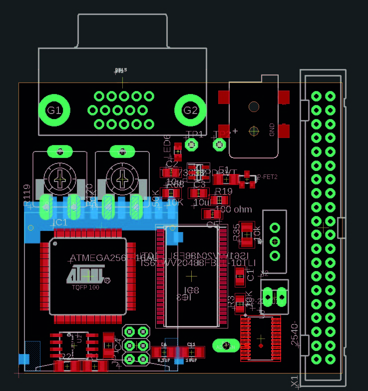
ATmega2560 SRAM board with SD card and I2C Flash memory. Raspberry pi as video in.
But not very interactive. More about messing with different kinds of memory, and as a parallel test as the FPGA but more familiar and constrained in C.
***
Don’t know what this is yet but, some kind of typology of memory modifications ?
![]()