Update:
- I can output HDMI video now
- I can now program the FPGA with raspberry pi
- I have finalized the all-logic, two board version of the béchamel and just need a Mouser order to put together the final version.
- After this béchamel 1 experience I have concluded that running a video synth operation developing with discrete logic chips would be so incredibly impractical (expensive, time consuming, physically large, inflexible) compared to working with reprogrammable logic like the FPGA.
- I want to finish this chapter of my project and then take a moment, to stop working, to think and to reflect. I either want to shift my attention to the preparedinstruments site, and trying to manage the making and selling of this board, or to take a break from electronics/programming research to read and explore elsewhere for a bit. I also want to show my project to people, like Vincent Rioux, and get their honest feedback about the meaning of this thing outside of my own interests and learning. I want to revisit my strategies and practices, how I work with lead solder and how I decide what boards to make. For instance, it was cool to design and produce lots of boards but it is inefficient when a single board that is just partially populated can do the work of various boards. Another thing : I have spent all this time testing stuff and have ended up with a board that is the same as everyone else’s : FPGA w/ SRAM, single board, rpi programmable. Should I start by doing things that other people are doing instead of trying to do everything else first ?
Update 2 :
Getting the SD card interfaced with FPGA isn’t a gimmick (like having an integrated screen, for instance) as it would make turn this object into a fully fledged “product” which isn’t reliant on another consumer product (like Arduino or rpi) to function. It makes sense to use an FPGA as Arduino cannot output HDMI, and is limited in terms of its ability to read an SD card, manage an SRAM, listen for buttons, and modify video simoultaneously. The system would be kind of complete with both large memory stockage, fast memory, input management, video output. But would it be fun to sell a product ? I would have to do do customer service, repairs, answer questions on the forum, handle shipping and customs. I think I would rather do art installations and kits / workshops ?
Recent Wintergatan youtube video suggested making explicit these :
- Problem definition : There is a lack of inexpensive, HDMI-compatible, live-playable, lo-fi hardware video synthesis devices on the synth market. But to be honest, this thing is not a response to a problem so much as a gratuitous problem-generating project (a.k.a a creative project).
- Design requirements : HDMI out, video in via SD card, USB-C power, tactile interface, (audio in ?). Live-playable, relatively small and light (to be easily shipped), inexpensive (~25 euros). Minimilist in design : no bloated software, everything implemented as simply and as fundamental/low-level as possible and everything using only 1,200 LUTs and 2MB of SRAM. On the other hand the device should be fun, quirky, expressive and playful in it’s output and physical incarnation. Everything on the board should be solderable by hand, nothing so small or specialized that you need special tools apart from a fine soldering iron.
I am working on a low-cost, NO SCHOOL NEVERS prototype that is just the Villette Makers PEW model with the addition of a small SRAM. This will be fun because I’ll be able to test the HDMI synth with memory and buttons. Before sending this design off to be made, I want to experiment more with SRAM and FPGA (to figure out what the smallest size memory I can get away with and if I should consider adding anything else to this board based on what I learn from these experiments).
- How can I record and playback with sync so images don’t jump around (taking H SYNC or Display Enable information in, presumably) ?
- How can I reduce the resolution of recordings (with clock divisions)?
- How can I record video to a single channel and mix several channels at output (put them on different colors is the easiest) ?
****
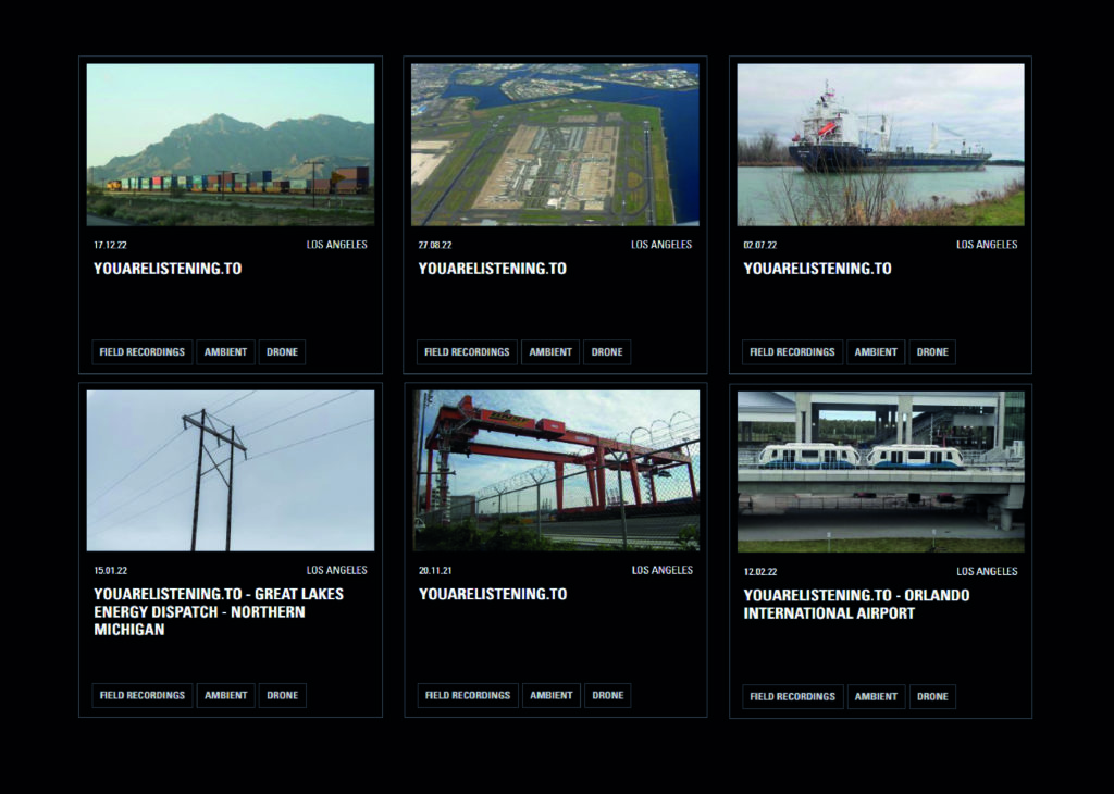
I mentioned Nosedrip, I also want to be able to make art like You Are Listening To. There is radio communication from various city systems like the train network, airports, waterways, etc. combined with ambient sounds.
****
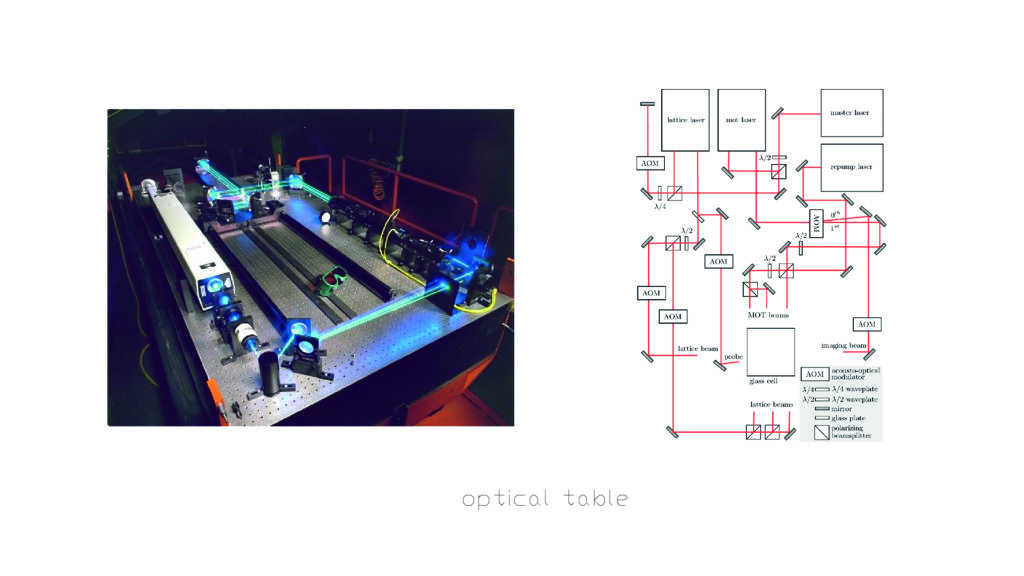
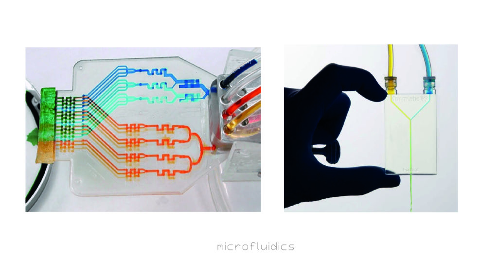
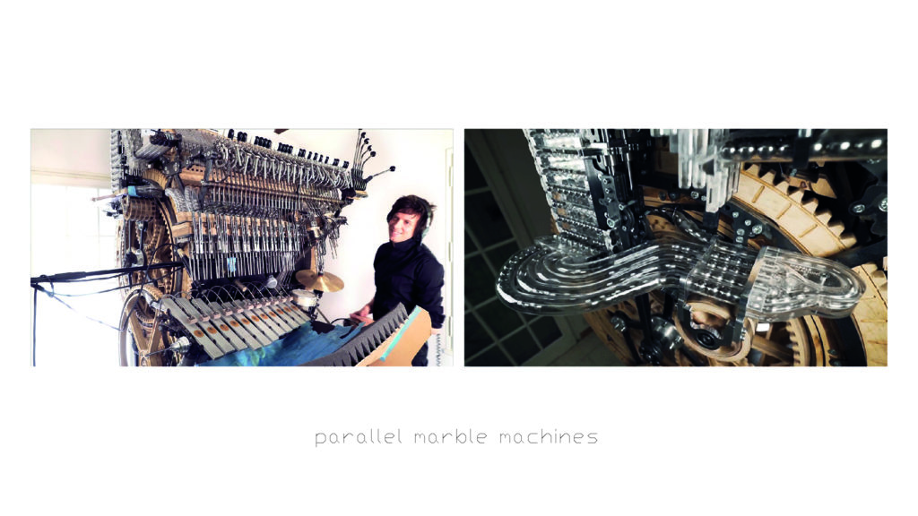
Working on slides for NO SCHOOL to explain what an FPGA is. Looking at some possible analogies. I can’t yet totally understand the difference between control flow programming (like in C) which performs one operation at a time (they digest?) and working with data flow pipelines that just kind of react (like a mirror or a lens) because of their form. I can’t tell if microfluidics and parallel marble machines are like FPGAs if you say that fluid moves super fast…
***
Trick to read analog signals with FPGA ( basically time how long it takes to charge a capacitor ) is genius : https://web.archive.org/web/20190615204217/https://hamsterworks.co.nz/mediawiki/index.php/Cheap_Analogue_Input * TO ADD TO NEXT BOARD*
***
In order to test SRAM recording, I’ve got the 4x16MB board back up and running. Here’s how I modified the board to get a test setup running :
- I took out the SD card from the previous RPI that was no longer appearing to output video from DPI. I have inserted it into a fresh raspberry pi and soldered a thinner profile 20×2 header “pi hat” (which makes the board less vulnerable to bending and losing connections).
- I desoldered the third and fourth SRAM chips (C&D) as they were causing issues for mysterious reasons I couldn’t debug. In any case I want to see what I can do with very little memory for the next board so not an issue.
- I replaced the PFET as I noticed before that it was getting hot and also that the power was fading after being initially plugged in.
- I removed the 50MHz oscillator on the board because it was unreliable and my attempts to resolder it just made it worse. So now it works with either rpi pixel clock or an external 25MHz from the function generator.
- I desoldered the two jumper wires I had soldered to access rpi_DEN & another non-connected rpi pin. All references to DEN have also been removed in the verilog.
There are two verilog codes which I’ve named vga_sync.v and vga_sync_test.v that need to be added :
/*
640x480 VGA singal generator
============================

- Creates h_sync,v_sync signals
- Creates display enable signal and horizontal, vertical
pixel position in display (h,v)
*/

`default_nettype none


module vga_sync(
input wire clk_in,
input wire reset,
output reg h_sync,
output reg v_sync,
output wire clk_sys,
output reg [11:0] h_count,
output reg [11:0] v_count,
output reg display_en
);


// Pixel counters
reg [11:0] h_counter = 0;
reg [11:0] v_counter = 0;

/*

//FOR 100MHz

localparam h_pixel_total = 3200;
localparam h_pixel_display = 2560;
localparam h_pixel_front_porch_amount = 64;
localparam h_pixel_sync_amount = 384;
localparam h_pixel_back_porch_amount = 192;

localparam v_pixel_total = 2100;
localparam v_pixel_display = 1920;
localparam v_pixel_front_porch_amount = 40;
localparam v_pixel_sync_amount = 8;
localparam v_pixel_back_porch_amount = 132;

*/

// FOR 50MHz

localparam h_pixel_total = 1600;
localparam h_pixel_display = 1280;
localparam h_pixel_front_porch_amount = 32;
localparam h_pixel_sync_amount = 192;
localparam h_pixel_back_porch_amount = 96;

localparam v_pixel_total = 1050;
localparam v_pixel_display = 960;
localparam v_pixel_front_porch_amount = 20;
localparam v_pixel_sync_amount = 4;
localparam v_pixel_back_porch_amount = 66;


/*

//FOR 25MHz

localparam h_pixel_total = 800;
localparam h_pixel_display = 640;
localparam h_pixel_front_porch_amount = 16;
localparam h_pixel_sync_amount = 96;
localparam h_pixel_back_porch_amount = 48;

localparam v_pixel_total = 525;
localparam v_pixel_display = 480;
localparam v_pixel_front_porch_amount = 10;
localparam v_pixel_sync_amount = 2;
localparam v_pixel_back_porch_amount = 33;

*/

always @(posedge clk_in) begin

if (reset) begin
//Reset counter values
h_counter <= 0;
v_counter <= 0;
display_en <= 0;
end
else
begin
// Generate display enable signal
if (h_counter < h_pixel_display && v_counter < v_pixel_display)
display_en <= 1;
else
display_en <= 0;

//Check if horizontal has arrived to the end
if (h_counter >= h_pixel_total)
begin
h_counter <= 0;
v_counter <= v_counter + 1;
end
else
//horizontal increment pixel value
h_counter <= h_counter + 1;
// check if vertical has arrived to the end
if (v_counter >= v_pixel_total)
v_counter <= 0;
end
end

always @(posedge clk_in) begin
// Check if sync_pulse needs to be created
if (h_counter >= (h_pixel_display + h_pixel_front_porch_amount)
&& h_counter < (h_pixel_display + h_pixel_front_porch_amount + h_pixel_sync_amount) )
h_sync <= 0;
else
h_sync <= 1;
// Check if sync_pulse needs to be created
if (v_counter >= (v_pixel_display + v_pixel_front_porch_amount)
&& v_counter < (v_pixel_display + v_pixel_front_porch_amount + v_pixel_sync_amount) )
v_sync <= 0;
else
v_sync <= 1;
end

// Route h_/v_counter to out
always @ (posedge clk_in) begin
h_count <= h_counter;
v_count <= v_counter;
end

endmodule
*****************************************************************************************************************************
// vga_sync_test verilog code

`default_nettype none

module vga_sync_test(

input wire clk_in,
input wire reset,

input wire rec, // Direction of io, 1 = set output, 0 = read input

//RASPBERRY PI
input wire [3:0] r_in,
input wire [3:0] b_in,
input wire [3:0] g_in,

//VGA OUT
output reg [3:0] r_out,
output reg [3:0] b_out,
output reg [3:0] g_out,

output wire h_sync,
output wire v_sync,

//SRAM

output reg [20:0] addr,
inout wire [7:0] io, // inout must be type wire

output wire cs_1,
output wire cs_0,

output reg we_1,
output reg we_0

);

wire [7:0] data_in;
wire [7:0] data_out;

reg toggle;

reg [7:0] a, b;

assign io = rec ? a : 8'bzzzzzzzz;

assign data_out = b;

assign data_in[1:0] = r_in[3:2];
assign data_in[3:2] = b_in[3:2];
assign data_in[5:4] = g_in[3:2];
assign data_in[7:6] = 2'b00;


wire display_en;
wire [11:0] h_count;
wire [11:0] v_count;

localparam h_pixel_max = 1280;
localparam v_pixel_max = 960;
localparam h_pixel_half = 640;
localparam v_pixel_half = 480;

// CS: low to select, high to deselect

assign cs_0 = toggle ? 1 : 0;
assign cs_1 = toggle ? 0 : 1;

//SRAM address counter

always @(posedge clk_in) begin

if (addr == 0) begin
toggle <= toggle+1;
end

if (reset) begin
addr <= 0;
end else begin
addr <= addr+1;
end
end

//REC control

always @(posedge clk_in) begin

b <= io;
a <= data_in;
if (rec) begin
we_0 <= addr[0]; //not sure why it isn't the inverse of addr[0] but that doesn't make the inverse on 'scope
end
else begin
we_0 <= 1;
end
end

//VGA COLOR OUT

always @(posedge clk_in) begin
if (display_en) begin

r_out[3:2] <= data_out[1:0];
r_out[1:0] <= data_out[1:0];
g_out[3:2] <= data_out[3:2];
g_out[1:0] <= data_out[3:2];
b_out[3:2] <= data_out[5:4];
b_out[1:0] <= data_out[5:4];

end else begin
r_out <= 4'b0000;
g_out <= 4'b0000;
b_out <= 4'b0000;
end
end

vga_sync vga_s(
.clk_in(clk_in),
.reset(reset),
.h_sync(h_sync),
.v_sync(v_sync),
.h_count(h_count),
.v_count(v_count),
.display_en(display_en) // '1' => pixel region
);

endmoduleset_io v_sync 87
set_io h_sync 88
set_io clk_in 64
set_io reset 66
set_io io[0] 1
set_io io[1] 2
set_io io[2] 3
set_io io[3] 4
set_io io[4] 122
set_io io[5] 121
set_io io[6] 120
set_io io[7] 119
set_io addr[0] 138
set_io addr[1] 139
set_io addr[2] 141
set_io addr[3] 142
set_io addr[4] 143
set_io addr[5] 8
set_io addr[6] 9
set_io addr[7] 10
set_io addr[8] 11
set_io addr[9] 12
set_io addr[10] 136
set_io addr[11] 135
set_io addr[12] 134
set_io addr[13] 129
set_io addr[14] 128
set_io addr[15] 117
set_io addr[16] 116
set_io addr[17] 115
set_io addr[18] 114
set_io addr[19] 137
set_io addr[20] 113
set_io cs_0 144
set_io cs_1 71
set_io we_0 7
set_io we_1 50
set_io rec 62
set_io r_in[0] 107
set_io r_in[1] 106
set_io r_in[2] 105
set_io r_in[3] 104
set_io g_in[0] 97
set_io g_in[1] 96
set_io g_in[2] 95
set_io g_in[3] 112
set_io b_in[0] 102
set_io b_in[1] 101
set_io b_in[2] 99
set_io b_in[3] 98
set_io r_out[0] 81
set_io r_out[1] 80
set_io r_out[2] 79
set_io r_out[3] 78
set_io g_out[0] 94
set_io g_out[1] 93
set_io g_out[2] 91
set_io g_out[3] 90
set_io b_out[0] 76
set_io b_out[1] 75
set_io b_out[2] 74
set_io b_out[3] 73
**************************************************************************************************************************
I describe here how I loaded videos to the rpi and setup the .desktop autorun code :

"Setting up another rpi to loop VLC videos" from https://www.marrs.io/la-bechamel/

Here is the raspberry pi config file I've used to get DPI working:
# For more options and information see
# http://rpf.io/configtxt
# Some settings may impact device functionality. See link above for details

# uncomment if you get no picture on HDMI for a default "safe" mode
#hdmi_safe=1

# uncomment the following to adjust overscan. Use positive numbers if console
# goes off screen, and negative if there is too much border
#overscan_left=16
#overscan_right=16
#overscan_top=16
#overscan_bottom=16

# uncomment to force a console size. By default it will be display's size minus
# overscan.
#framebuffer_width=1280
#framebuffer_height=720

# uncomment if hdmi display is not detected and composite is being output
#hdmi_force_hotplug=1

# uncomment to force a specific HDMI mode (this will force VGA)
#hdmi_group=1
#hdmi_mode=1

# uncomment to force a HDMI mode rather than DVI. This can make audio work in
# DMT (computer monitor) modes
#hdmi_drive=2

# uncomment to increase signal to HDMI, if you have interference, blanking, or
# no display
#config_hdmi_boost=4

# uncomment for composite PAL
#sdtv_mode=2

#uncomment to overclock the arm. 700 MHz is the default.
#arm_freq=800

# Uncomment some or all of these to enable the optional hardware interfaces
dtparam=i2c_arm=off
#dtparam=i2s=on
dtparam=spi=off

# Uncomment this to enable infrared communication.
#dtoverlay=gpio-ir,gpio_pin=17
#dtoverlay=gpio-ir-tx,gpio_pin=18

# Additional overlays and parameters are documented /boot/overlays/README

# Enable audio (loads snd_bcm2835)
dtparam=audio=on

# Automatically load overlays for detected cameras
camera_auto_detect=1

# Automatically load overlays for detected DSI displays
#display_auto_detect=1

# Enable DRM VC4 V3D driver
#dtoverlay=vc4-kms-v3d
max_framebuffers=2

# Disable compensation for displays with overscan
disable_overscan=1

[cm4]
# Enable host mode on the 2711 built-in XHCI USB controller.
# This line should be removed if the legacy DWC2 controller is required
# (e.g. for USB device mode) or if USB support is not required.
otg_mode=1

[all]

[pi4]
# Run as fast as firmware / board allows
arm_boost=1

[all]

gpio=0-9=a2
gpio=12-17=a2
gpio=20-25=a2
gpio=26-27=a2

dtoverlay=dpi24

enable_dpi_lcd=1
display_default_lcd=1

dpi_group=2
dpi_mode=87

extra_transpose_buffer=2

dpi_output_format=0x7f216
dpi_timings=720 0 40 48 128 720 0 13 3 15 0 0 0 60 0 50000000 1
******
- How can I record and playback with sync so images don’t jump around (taking H SYNC or Display Enable information in, presumably) ?
- How can I reduce the resolution of recordings (with clock divisions)?
- How can I record video to a single channel and mix several channels at output (put them on different colors is the easiest) ?
SYNC
I have tried using Data Enable (DEN) from the rpi and inputting that, and also using H_SYNC and V_SYNC from the r_pi. So far the best result is taking V_SYNC, but I am still getting drifting. Testing to see if both H_SYNC and V_SYNC are high isn’t more stable for some reason. Here is that code :
`default_nettype none

module vga_sync_test(

input wire clk_in,
input wire reset,

input wire rec, // Direction of io, 1 = set output, 0 = read input

//RASPBERRY PI
input wire [3:0] r_in,
input wire [3:0] b_in,
input wire [3:0] g_in,

input wire DEN,


//VGA OUT
output reg [3:0] r_out,
output reg [3:0] b_out,
output reg [3:0] g_out,

output wire h_sync,
output wire v_sync,

//SRAM

output reg [20:0] addr,
inout wire [7:0] io, // inout must be type wire

output wire cs_1,
output wire cs_0,

output reg we_1,
output reg we_0

);

wire [7:0] data_in;
wire [7:0] data_out;

reg toggle;

reg [7:0] a, b;

assign io = rec ? a : 8'bzzzzzzzz;

assign data_out = b;

assign data_in[1:0] = DEN ? r_in[3:2] : 0;

assign data_in[1:0] = DEN ? r_in[3:2] : 0;
assign data_in[3:2] = DEN ? b_in[3:2] : 0;
assign data_in[5:4] = DEN ? g_in[3:2] : 0;
assign data_in[7:6] = 2'b00;


wire display_en;
wire [11:0] h_count;
wire [11:0] v_count;

localparam h_pixel_max = 1280;
localparam v_pixel_max = 960;
localparam h_pixel_half = 640;
localparam v_pixel_half = 480;

// CS: low to select, high to deselect

assign cs_0 = toggle ? 1 : 0;
assign cs_1 = toggle ? 0 : 1;

//SRAM address counter

always @(posedge clk_in) begin

if (addr == 0) begin
toggle <= toggle+1;
end

if (reset) begin
addr <= 0;
end else begin

//only increment address is DEN high
if (DEN) begin
addr <= addr+1;
end
end
end

//REC control

always @(posedge clk_in) begin

b <= io;
a <= data_in;
if (rec) begin

//only enable WR if DEN high
if (DEN) begin
we_0 <= addr[0]; //not sure why it isn't the inverse of addr[0] but that doesn't make the inverse on 'scope
end
end
else begin
we_0 <= 1;
end
end

//VGA COLOR OUT

always @(posedge clk_in) begin

//only display pixels if DEN high
if (DEN) begin

r_out[3:2] <= data_out[1:0];
r_out[1:0] <= data_out[1:0];
g_out[3:2] <= data_out[3:2];
g_out[1:0] <= data_out[3:2];
b_out[3:2] <= data_out[5:4];
b_out[1:0] <= data_out[5:4];

end else begin
r_out <= 4'b0000;
g_out <= 4'b0000;
b_out <= 4'b0000;
end
end

vga_sync vga_s(
.clk_in(clk_in),
.reset(reset),
.h_sync(h_sync),
.v_sync(v_sync),
.h_count(h_count),
.v_count(v_count),
.display_en(display_en) // '1' => pixel region
);

endmodule
I am going to try to count V_SYNCs and use this to vary SRAM address incrementing.
I can get an image to freeze pretty well now, I just needed to find the right size of the V_SYNC_COUNT counter to make it work. Here is the code :
`default_nettype none

module vga_sync_test(

input wire clk_in,
input wire reset,

input wire rec, // Direction of io, 1 = set output, 0 = read input

//RASPBERRY PI
input wire [3:0] r_in,
input wire [3:0] b_in,
input wire [3:0] g_in,

input wire DEN,
output reg [2:0] V_SYNC_COUNT, // the size of this counter impact how many V_SYNC signals it takes to reset the SRAM ADD counter


//VGA OUT
output reg [3:0] r_out,
output reg [3:0] b_out,
output reg [3:0] g_out,

output wire h_sync,
output wire v_sync,

//SRAM

output reg [20:0] addr,
inout wire [7:0] io, // inout must be type wire

output wire cs_1,
output wire cs_0,

output reg we_1,
output reg we_0

);

wire [7:0] data_in;
wire [7:0] data_out;

reg toggle;

reg [7:0] a, b;

assign io = rec ? a : 8'bzzzzzzzz;

assign data_out = b;

assign data_in[1:0] = DEN ? r_in[3:2] : 0;

assign data_in[1:0] = DEN ? r_in[3:2] : 0;
assign data_in[3:2] = DEN ? b_in[3:2] : 0;
assign data_in[5:4] = DEN ? g_in[3:2] : 0;
assign data_in[7:6] = 2'b00;


wire display_en;
wire [11:0] h_count;
wire [11:0] v_count;

localparam h_pixel_max = 1280;
localparam v_pixel_max = 960;
localparam h_pixel_half = 640;
localparam v_pixel_half = 480;

// CS: low to select, high to deselect

assign cs_0 = toggle ? 1 : 0;
assign cs_1 = toggle ? 0 : 1;

//V SYNC counter

always @(posedge DEN) begin
V_SYNC_COUNT <= V_SYNC_COUNT+1;
if(reset == 1) begin
V_SYNC_COUNT <=0;
end
end


//SRAM address counter

always @(posedge clk_in) begin

if (addr == 0) begin
toggle <= toggle+1;
end

// reset the address once we've rolled over V_SYNC_COUNT

if (reset | V_SYNC_COUNT == 0 ) begin
addr <= 0;
end else begin

//only increment address is DEN high
if (DEN) begin
addr <= addr+1;
end
end
end

//REC control

always @(posedge clk_in) begin

b <= io;
a <= data_in;
if (rec) begin

//only enable WR if DEN high
if (DEN) begin
we_0 <= addr[0]; //not sure why it isn't the inverse of addr[0] but that doesn't make the inverse on 'scope
end
end
else begin
we_0 <= 1;
end
end

//VGA COLOR OUT

always @(posedge clk_in) begin

//only display pixels if DEN high
if (DEN) begin

r_out[3:2] <= data_out[1:0];
r_out[1:0] <= data_out[1:0];
g_out[3:2] <= data_out[3:2];
g_out[1:0] <= data_out[3:2];
b_out[3:2] <= data_out[5:4];
b_out[1:0] <= data_out[5:4];

end else begin
r_out <= 4'b0000;
g_out <= 4'b0000;
b_out <= 4'b0000;
end
end

vga_sync vga_s(
.clk_in(clk_in),
.reset(reset),
.h_sync(h_sync),
.v_sync(v_sync),
.h_count(h_count),
.v_count(v_count),
.display_en(display_en) // '1' => pixel region
);

endmodule
I just realized I could also take the AND of various bits of the V_SYNC_COUNTER like so :
if (reset | ((V_SYNC_COUNT[0] == 1) & (V_SYNC_COUNT[2] == 1) & (V_SYNC_COUNT[3] == 1))) begin

addr <= 0;

end
RESOLUTION
This is cool, just change clk_in with a divided clock and you get bigger pixels !
`default_nettype none

module vga_sync_test(

input wire clk_in,

output reg [2:0] clk_div, // remember to change clk_div[MSB] also below ! Changing the size of this register changes how big the pixels are :D !

input wire reset,

input wire rec, // Direction of io, 1 = set output, 0 = read input

//RASPBERRY PI
input wire [3:0] r_in,
input wire [3:0] b_in,
input wire [3:0] g_in,

input wire DEN,
output reg [1:0] V_SYNC_COUNT,


//VGA OUT
output reg [3:0] r_out,
output reg [3:0] b_out,
output reg [3:0] g_out,

output wire h_sync,
output wire v_sync,

//SRAM

output reg [20:0] addr,
inout wire [7:0] io, // inout must be type wire

output wire cs_1,
output wire cs_0,

output reg we_1,
output reg we_0

);

wire [7:0] data_in;
wire [7:0] data_out;

reg toggle;

reg [7:0] a, b;

assign io = rec ? a : 8'bzzzzzzzz;

assign data_out = b;

assign data_in[1:0] = DEN ? r_in[3:2] : 0;

assign data_in[1:0] = DEN ? r_in[3:2] : 0;
assign data_in[3:2] = DEN ? b_in[3:2] : 0;
assign data_in[5:4] = DEN ? g_in[3:2] : 0;
assign data_in[7:6] = 2'b00;


wire display_en;
wire [11:0] h_count;
wire [11:0] v_count;

localparam h_pixel_max = 1280;
localparam v_pixel_max = 960;
localparam h_pixel_half = 640;
localparam v_pixel_half = 480;

// CS: low to select, high to deselect

assign cs_0 = toggle ? 1 : 0;
assign cs_1 = toggle ? 0 : 1;

//V SYNC counter

always @(posedge DEN) begin
V_SYNC_COUNT <= V_SYNC_COUNT+1;
if(reset == 1) begin
V_SYNC_COUNT <=0;
end
end

//increment our clock divider

always @(posedge clk_in) begin
clk_div <= clk_div+1;
if(reset == 1) begin
clk_div <=0;
end
end

//SRAM address counter

always @(posedge clk_div[1]) begin

if (addr == 0) begin
toggle <= toggle+1;
end

// reset the address once we've rolled over V_SYNC_COUNT

if (reset | V_SYNC_COUNT == 0 ) begin
addr <= 0;
end else begin

//only increment address if DEN high
if (DEN) begin
addr <= addr+1;
end
end
end

//REC control

always @(posedge clk_div[1]) begin

b <= io;
a <= data_in;
if (rec) begin

//only enable WR if DEN high
if (DEN) begin
we_0 <= addr[0]; //not sure why it isn't the inverse of addr[0] but that doesn't make the inverse on 'scope
end
end
else begin
we_0 <= 1;
end
end

//VGA COLOR OUT

always @(posedge clk_div[1]) begin

//only display pixels if DEN high
if (DEN) begin

r_out[3:2] <= data_out[1:0];
r_out[1:0] <= data_out[1:0];
g_out[3:2] <= data_out[3:2];
g_out[1:0] <= data_out[3:2];
b_out[3:2] <= data_out[5:4];
b_out[1:0] <= data_out[5:4];

end else begin
r_out <= 4'b0000;
g_out <= 4'b0000;
b_out <= 4'b0000;
end
end

vga_sync vga_s(
.clk_in(clk_in),
.reset(reset),
.h_sync(h_sync),
.v_sync(v_sync),
.h_count(h_count),
.v_count(v_count),
.display_en(display_en) // '1' => pixel region
);

endmodule
![]()
Considering removing the amps at the output, as the NO SCHOOL version won’t have these either.
I should definitely change the shape of the pixels to make them rectangular in both X and Y.
**********
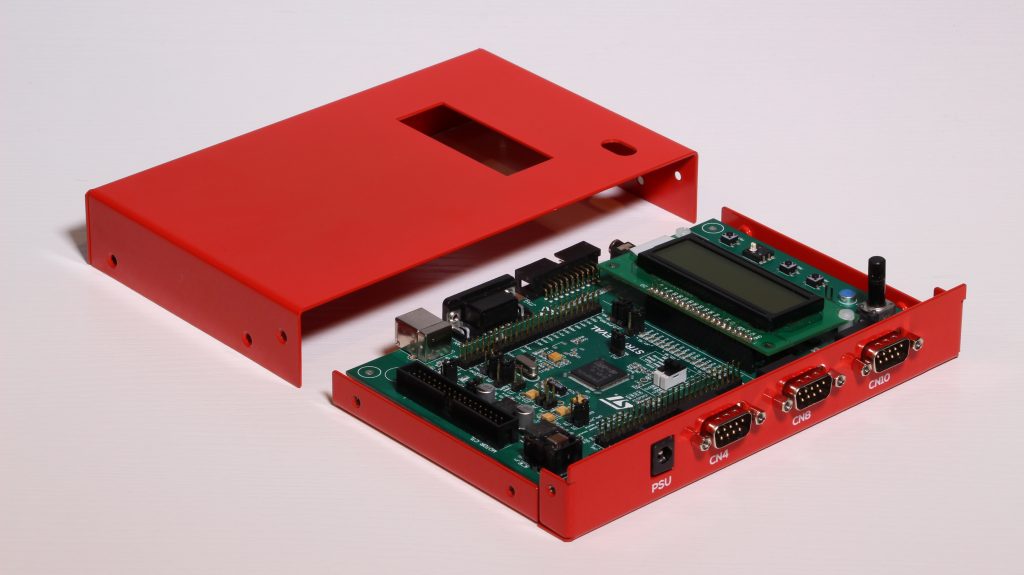
I might be entering a new career phase as a prototyper. I am currently working to make an e-ink QR code device, a rotating clock mechanism, and may be tasked with making permanent versions of the FLV DSAA prototypes we proposed !
I can imagine a transition where I do more prototyping professionally and spend my time doing more fine art work – less design of circuits and more experimental video making with my existing boards + new code. Routing circuits is so meticulous, I don’t know how I’ve spent so many hours doing this.
**************
I have finalized the next iteration of the PEW board with a small inexpensive 2MB SRAM, an rpi header (which is also hard-wired to the FLASH programming pins), and an SD card set up to work in either 1 or 4 bit mode (not SPI0) to eventually take in uncompressed video directly, and a test of the potentiometer reading capabilities of the FPGA. The music in + comparator has been removed from this version. I also haven’t been able to learn quickly enough a minimal setup for the FTDI chip so that has not been included either.
I have soldered the first test board :
Experimented with round keys…not sure it’s a keeper.
HDMI is working :
Strange issue that I have faced before : I need to press down on the clock, FPGA or flash memory to get it working…
Fabien’s super flux is making a world of difference, it was hard not to solder perfectly.
The HDMI USB recorder works super well with OBS, and is less hassle than the VGA recorder by far.
To keep in mind for the NO SCHOOL board :
- Include the 3 SEL BITs to make three different codes possible
- Have the resistors always in the same configuration for the VGA colors
- Always have the same pattern for the 1K, 10K, and 0.1uF for the keys
- Reorder green LEDs
- The VGA plugs I ordered for this kit are mirrored or the footprint is mirrored ?
Here is the verilog code I set up to test the buttons :
`default_nettype none // disable implicit definitions by Verilog
//-----------------------------------------------------------------
// minimalDVID_encoder.vhd : A quick and dirty DVI-D implementation
//
// Author: Mike Field <hamster@snap.net.nz>
//
// DVI-D uses TMDS as the 'on the wire' protocol, where each 8-bit
// value is mapped to one or two 10-bit symbols, depending on how
// many 1s or 0s have been sent. This makes it a DC balanced protocol,
// as a correctly implemented stream will have (almost) an equal
// number of 1s and 0s.
//
// Because of this implementation quite complex. By restricting the
// symbols to a subset of eight symbols, all of which having have
// five ones (and therefore five zeros) this complexity drops away
// leaving a simple implementation. Combined with a DDR register to
// send the symbols the complexity is kept very low.
//-----------------------------------------------------------------

module top(
clk100, key, hdmi_p, hdmi_n
);

input clk100;
input wire key[8:0],
output [3:0] hdmi_p;
output [3:0] hdmi_n;

// For holding the outward bound TMDS symbols in the slow and fast domain
reg [9:0] c0_symbol; reg [9:0] c0_high_speed;
reg [9:0] c1_symbol; reg [9:0] c1_high_speed;
reg [9:0] c2_symbol; reg [9:0] c2_high_speed;
reg [9:0] clk_high_speed;

reg [1:0] c2_output_bits;
reg [1:0] c1_output_bits;
reg [1:0] c0_output_bits;
reg [1:0] clk_output_bits;

wire clk_x5;
reg [2:0] latch_high_speed = 3'b100; // Controlling the transfers into the high speed domain

wire vsync, hsync;
wire [1:0] syncs; // To glue the HSYNC and VSYNC into the control character
assign syncs = {vsync, hsync};

// video structure constants
parameter hpixels = 800; // horizontal pixels per line
parameter vlines = 525; // vertical lines per frame
parameter hpulse = 96; // hsync pulse length
parameter vpulse = 2; // vsync pulse length
parameter hbp = 144; // end of horizontal back porch (96 + 48)
parameter hfp = 784; // beginning of horizontal front porch (800 - 16)
parameter vbp = 35; // end of vertical back porch (2 + 33)
parameter vfp = 515; // beginning of vertical front porch (525 - 10)

// registers for storing the horizontal & vertical counters
reg [9:0] vc;
reg [9:0] hc;
// generate sync pulses (active high)
assign vsync = (vc < vpulse);
assign hsync = (hc < hpulse);

always @(posedge clk_x5) begin
//-------------------------------------------------------------
// Now take the 10-bit words and take it into the high-speed
// clock domain once every five cycles.
//
// Then send out two bits every clock cycle using DDR output
// registers.
//-------------------------------------------------------------
c0_output_bits <= c0_high_speed[1:0];
c1_output_bits <= c1_high_speed[1:0];
c2_output_bits <= c2_high_speed[1:0];
clk_output_bits <= clk_high_speed[1:0];
if (latch_high_speed[2]) begin // pixel clock 25MHz
c0_high_speed <= c0_symbol;
c1_high_speed <= c1_symbol;
c2_high_speed <= c2_symbol;
clk_high_speed <= 10'b0000011111;
latch_high_speed <= 3'b000;
if (hc < hpixels)
hc <= hc + 1;
else
begin
hc <= 0;
if (vc < vlines)
vc <= vc + 1;
else
vc <= 0;
end
end
else begin
c0_high_speed <= {2'b00, c0_high_speed[9:2]};
c1_high_speed <= {2'b00, c1_high_speed[9:2]};
c2_high_speed <= {2'b00, c2_high_speed[9:2]};
clk_high_speed <= {2'b00, clk_high_speed[9:2]};
latch_high_speed <= latch_high_speed + 1'b1;
end
end

always @(*) // display 100% saturation colourbars
begin
// first check if we're within vertical active video range
if (vc >= vbp && vc < vfp)
begin
// now display different colours every 80 pixels
// while we're within the active horizontal range
// based on which buttons are pressed
// -----------------
// display white bar

if (key[0] == 0 && hc >= hbp && hc < (hbp+80))
begin
c2_symbol = 10'b1011110000; // red
c1_symbol = 10'b1011110000; // green
c0_symbol = 10'b1011110000; // blue
end
// display yellow bar
else if (key[1] == 0 && hc >= (hbp+80) && hc < (hbp+160))
begin
c2_symbol = 10'b1011110000; // red
c1_symbol = 10'b1011110000; // green
c0_symbol = 10'b0111110000; // blue
end
// display cyan bar
else if (key[2] == 0 && hc >= (hbp+160) && hc < (hbp+240))
begin
c2_symbol = 10'b0111110000; // red
c1_symbol = 10'b1011110000; // green
c0_symbol = 10'b1011110000; // blue
end
// display green bar
else if (key[3] == 0 && hc >= (hbp+240) && hc < (hbp+320))
begin
c2_symbol = 10'b0111110000; // red
c1_symbol = 10'b1011110000; // green
c0_symbol = 10'b0111110000; // blue
end
// display magenta bar
else if (key[4] == 0 && hc >= (hbp+320) && hc < (hbp+400))
begin
c2_symbol = 10'b1011110000; // red
c1_symbol = 10'b0111110000; // green
c0_symbol = 10'b1011110000; // blue
end
// display red bar
else if (key[5] == 0 && hc >= (hbp+400) && hc < (hbp+480))
begin
c2_symbol = 10'b1011110000; // red
c1_symbol = 10'b0111110000; // green
c0_symbol = 10'b0111110000; // blue
end
// display blue bar
else if (key[6] == 0 && hc >= (hbp+480) && hc < (hbp+560))
begin
c2_symbol = 10'b0111110000; // red
c1_symbol = 10'b0111110000; // green
c0_symbol = 10'b1011110000; // blue
end
// display black bar
else if (key[7] == 0 && hc >= (hbp+560) && hc < hfp)
begin
c2_symbol = 10'b0111110000; // red
c1_symbol = 10'b0111110000; // green
c0_symbol = 10'b0111110000; // blue
end
// we're outside active horizontal range
else
begin
c2_symbol = 10'b1101010100; // red
c1_symbol = 10'b1101010100; // green
//---------------------------------------------
// Channel 0 carries the blue pixels, and also
// includes the HSYNC and VSYNCs during
// the CTL (blanking) periods.
//---------------------------------------------
case (syncs)
2'b00 : c0_symbol = 10'b1101010100;
2'b01 : c0_symbol = 10'b0010101011;
2'b10 : c0_symbol = 10'b0101010100;
default : c0_symbol = 10'b1010101011;
endcase
end
end
// we're outside active vertical range
else
begin
c2_symbol = 10'b1101010100; // red
c1_symbol = 10'b1101010100; // green
//---------------------------------------------
// Channel 0 carries the blue pixels, and also
// includes the HSYNC and VSYNCs during
// the CTL (blanking) periods.
//---------------------------------------------
case (syncs)
2'b00 : c0_symbol = 10'b1101010100;
2'b01 : c0_symbol = 10'b0010101011;
2'b10 : c0_symbol = 10'b0101010100;
default : c0_symbol = 10'b1010101011;
endcase
end
end

// red N
defparam hdmin2.PIN_TYPE = 6'b010000;
defparam hdmin2.IO_STANDARD = "SB_LVCMOS";
SB_IO hdmin2 (
.PACKAGE_PIN (hdmi_n[2]),
.CLOCK_ENABLE (1'b1),
.OUTPUT_CLK (clk_x5),
.OUTPUT_ENABLE (1'b1),
.D_OUT_0 (~c2_output_bits[1]),
.D_OUT_1 (~c2_output_bits[0])
);

// red P
defparam hdmip2.PIN_TYPE = 6'b010000;
defparam hdmip2.IO_STANDARD = "SB_LVCMOS";
SB_IO hdmip2 (
.PACKAGE_PIN (hdmi_p[2]),
.CLOCK_ENABLE (1'b1),
.OUTPUT_CLK (clk_x5),
.OUTPUT_ENABLE (1'b1),
.D_OUT_0 (c2_output_bits[1]),
.D_OUT_1 (c2_output_bits[0])
);

// green N
defparam hdmin1.PIN_TYPE = 6'b010000;
defparam hdmin1.IO_STANDARD = "SB_LVCMOS";
SB_IO hdmin1 (
.PACKAGE_PIN (hdmi_n[1]),
.CLOCK_ENABLE (1'b1),
.OUTPUT_CLK (clk_x5),
.OUTPUT_ENABLE (1'b1),
.D_OUT_0 (~c1_output_bits[1]),
.D_OUT_1 (~c1_output_bits[0])
);

// green P
defparam hdmip1.PIN_TYPE = 6'b010000;
defparam hdmip1.IO_STANDARD = "SB_LVCMOS";
SB_IO hdmip1 (
.PACKAGE_PIN (hdmi_p[1]),
.CLOCK_ENABLE (1'b1),
.OUTPUT_CLK (clk_x5),
.OUTPUT_ENABLE (1'b1),
.D_OUT_0 (c1_output_bits[1]),
.D_OUT_1 (c1_output_bits[0])
);


// blue N
defparam hdmin0.PIN_TYPE = 6'b010000;
defparam hdmin0.IO_STANDARD = "SB_LVCMOS";
SB_IO hdmin0 (
.PACKAGE_PIN (hdmi_n[0]),
.CLOCK_ENABLE (1'b1),
.OUTPUT_CLK (clk_x5),
.OUTPUT_ENABLE (1'b1),
.D_OUT_0 (~c0_output_bits[1]),
.D_OUT_1 (~c0_output_bits[0])
);

// blue P
defparam hdmip0.PIN_TYPE = 6'b010000;
defparam hdmip0.IO_STANDARD = "SB_LVCMOS";
SB_IO hdmip0 (
.PACKAGE_PIN (hdmi_p[0]),
.CLOCK_ENABLE (1'b1),
.OUTPUT_CLK (clk_x5),
.OUTPUT_ENABLE (1'b1),
.D_OUT_0 (c0_output_bits[1]),
.D_OUT_1 (c0_output_bits[0])
);

// clock N
defparam hdmin3.PIN_TYPE = 6'b010000;
defparam hdmin3.IO_STANDARD = "SB_LVCMOS";
SB_IO hdmin3 (
.PACKAGE_PIN (hdmi_n[3]),
.CLOCK_ENABLE (1'b1),
.OUTPUT_CLK (clk_x5),
.OUTPUT_ENABLE (1'b1),
.D_OUT_0 (~clk_output_bits[1]),
.D_OUT_1 (~clk_output_bits[0])
);


// clock P
defparam hdmip3.PIN_TYPE = 6'b010000;
defparam hdmip3.IO_STANDARD = "SB_LVCMOS";
SB_IO hdmip3 (
.PACKAGE_PIN (hdmi_p[3]),
.CLOCK_ENABLE (1'b1),
.OUTPUT_CLK (clk_x5),
.OUTPUT_ENABLE (1'b1),
.D_OUT_0 (clk_output_bits[1]),
.D_OUT_1 (clk_output_bits[0])
);
// D_OUT_0 and D_OUT_1 swapped?
// https://github.com/YosysHQ/yosys/issues/330


SB_PLL40_PAD #(
.FEEDBACK_PATH ("SIMPLE"),
.DIVR (4'b0000),
.DIVF (7'b0001001),
.DIVQ (3'b011),
.FILTER_RANGE (3'b101)
) uut (
.RESETB (1'b1),
.BYPASS (1'b0),
.PACKAGEPIN (clk100),
.PLLOUTGLOBAL (clk_x5) // DVI clock 125MHz
);

endmodule
Here is the pcf :
set_io hdmi_p[0] 139 -io_std SB_LVCMOS
set_io hdmi_p[2] 78 -io_std SB_LVCMOS
set_io hdmi_p[1] 80 -io_std SB_LVCMOS
set_io hdmi_p[3] 137 -io_std SB_LVCMOS
set_io hdmi_n[0] 138 -io_std SB_LVCMOS
set_io hdmi_n[2] 79 -io_std SB_LVCMOS
set_io hdmi_n[1] 81 -io_std SB_LVCMOS
set_io hdmi_n[3] 136 -io_std SB_LVCMOS

set_io key[0] 37
set_io key[1] 38
set_io key[2] 39
set_io key[3] 41
set_io key[4] 42
set_io key[5] 43
set_io key[6] 44
set_io key[7] 45
set_io key[8] 47
set_io clk100 49
Makes some nice buggy HDMI images :


**************
UPDATE : It appears that SPI mode, not SD 1-bit mode, is the more thoroughly documented way of interfacing SD cards.
Here is where the SD 1-bit mode communication protocol is explained : https://www.sdcard.org/downloads/pls/ and select Physical Layer Simplified Specification where chapter 4 describes in detail.
I think I should aim for the Multiple Block Read Operation (CMD18) which keeps going until you send a stop command. 1 bit mode seems the simplest, everything is just in serial.
Here are some sample diagrams :
*************************
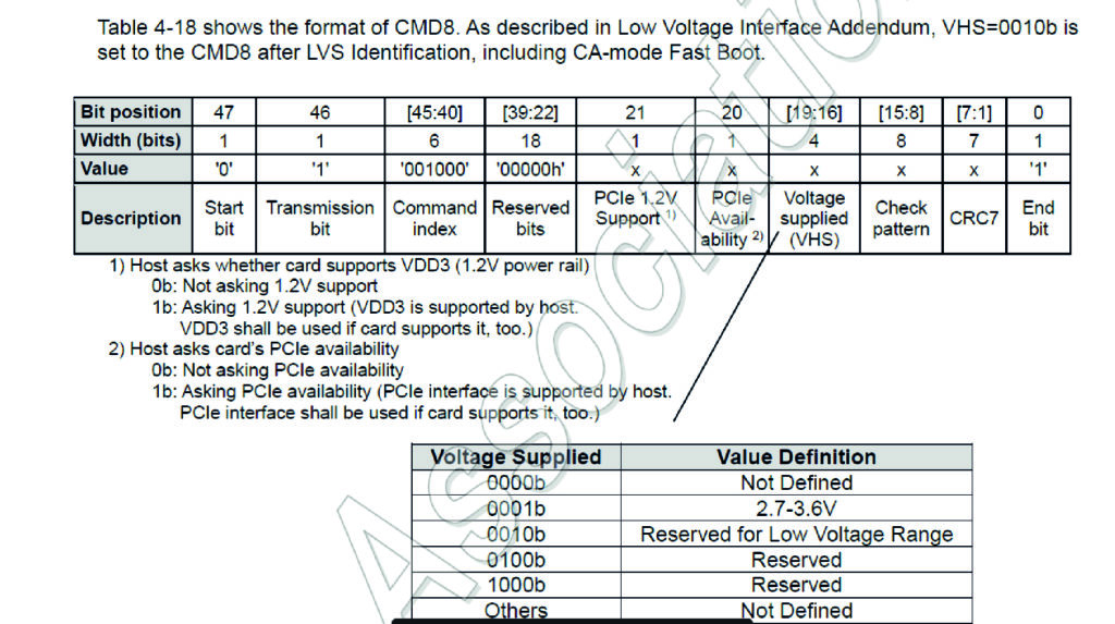
General stuff : CMD is used for sending messages, DAT0 for sending data. 3.3V is the standard. Default clock speed is 400KHz, default RCA is 0x0000. Phase 1 is Card ID mode then Data TX mode. 512 bytes sent at a time. According to this post (http://forum.6502.org/viewtopic.php?f=4&t=7300) data is read on the low-to-high transition, and starts with the highest bit (47, for example) going to the lowest bit. Here is a site to calculate CRC (https://www.lddgo.net/en/encrypt/crc)
Here is my, so far successful, attempt directly copying the messages sent here (http://forum.6502.org/viewtopic.php?f=4&t=7300) :
//-----------------------------------------------------------------
// Attempt at SD 1 bit communication
//-----------------------------------------------------------------

`default_nettype none // disable implicit definitions by Verilog

module top(
input wire clk100,
input wire reset,
output reg SCK,
output reg CMD,
output wire LED1,
output wire LED5
);

//some counters
reg [9:0] counter=0;
reg [9:0] q=0;

reg half_sec_pulse = 0;

assign LED1 = half_sec_pulse;
assign LED5 = half_sec_pulse;

reg[25:0] div_cntr1;
reg[25:0] div_cntr2;

always@(posedge clk100)
begin

div_cntr1 <= div_cntr1 + 1;
if (div_cntr1 == 0)
if (div_cntr2 == 0)
begin
div_cntr2 <= 0;
half_sec_pulse <= ~half_sec_pulse;
end

else
div_cntr2 <= div_cntr2 + 1;
else
half_sec_pulse <= half_sec_pulse;
end


// divide 100MHz clock by 1024 to equal 97.65625 KHz (but I'm seeing half that on the 'scope)

always @(posedge clk100) begin

q <= q+1;
if(q == 0) begin
SCK <= ~SCK;
end
end

//start with 80 clock ticks while CMD high

always @(posedge SCK) begin
//wait a half second after power up
if(half_sec_pulse==1)begin
//only do all this one time
counter <= (counter==400) ? counter : counter+1;

if (counter <= 79) begin
CMD <= 1;
end

//send CMD0

if ((counter > 79) && (counter <= 128)) begin

if(counter==81||counter==120||counter==123||counter==125||counter==127||counter==128)begin
CMD <= 1;
end
else begin
CMD <= 0;
end
end

//send 80 clock ticks while CMD high

if ((counter > 129) && (counter <= 209)) begin
CMD <= 1;
end


//send CMD8
if ((counter > 209) && (counter <= 257)) begin

if(counter==211||counter==214||counter==241||counter==242||counter==244||counter==246||counter==248||counter==250||counter==255||counter==256||counter==257)begin
CMD <= 1;
end
else begin
CMD <= 0;
end
end

//set CMD to input and listen !
if ((counter > 257) && (counter <= 400)) begin

CMD <= 1'bz; // put in high Z
end

end
end
endmodule
Here is the pcf :
set_io hdmi_p[0] 139 -io_std SB_LVCMOS
set_io hdmi_p[2] 78 -io_std SB_LVCMOS
set_io hdmi_p[1] 80 -io_std SB_LVCMOS
set_io hdmi_p[3] 137 -io_std SB_LVCMOS
set_io hdmi_n[0] 138 -io_std SB_LVCMOS
set_io hdmi_n[2] 79 -io_std SB_LVCMOS
set_io hdmi_n[1] 81 -io_std SB_LVCMOS
set_io hdmi_n[3] 136 -io_std SB_LVCMOS
set_io key[0] 37
set_io key[1] 38
set_io key[2] 39
set_io key[3] 41
set_io key[4] 42
set_io key[5] 43
set_io key[6] 44
set_io key[7] 45
set_io key[8] 47
set_io SCK 32
set_io CMD 33
set_io LED1 29
set_io LED5 28
set_io reset 66
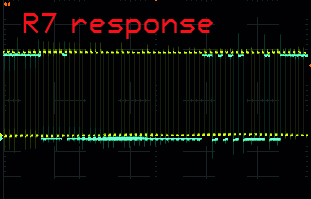
set_io clk100 49This works, thanks to this post for all the answers and detailed oscilloscope screen shots from AndrewP and John West on this forum : http://forum.6502.org/viewtopic.php?f=4&t=7300

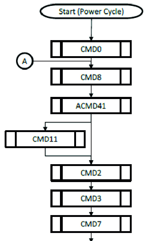
And I’m following this overall sequence :
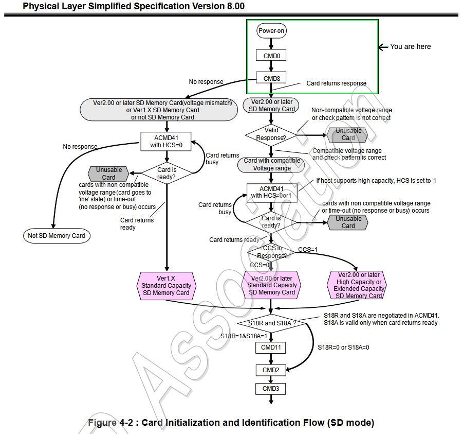
John West writes that the steps are :
- CMD0 “GO_IDLE_STATE”
- CMD8 “SEND_IF_COND”
- CMD55 “APP_CMD”, ACMD41 “SD_SEND_OP_COND” with argument 40100000 (HCS=1, voltage = 3.3). The R3 response has HCS and the supported voltages set. Repeat until bit 31 of the response is 1.
- CMD2 “ALL_SEND_CID” with argument 00000000. The R2 response has the CID. I ignore it.
- CMD3 “SEND_RELATIVE_ADDR” with argument 00000000. The R6 response contains the RCA and some status that I ignore.
The card is now in the stand-by state. Reading a block is accomplished by
- CMD7 “SELECT/DESELECT_CARD” with argument bits 31-16 = the RCA you were given, 15-0 = 0. The R1b response I ignore.
- CMD17 “READ_SINGLE_BLOCK” with argument = the block address. The R1 response I ignore, but there will also be the block data. Keep toggling the clock, and you’ll eventually see a start bit followed by a block of data and a CRC.
Here is the start-up procedure :
**********************
Card ID mode: After power on, the Host sends to the SD card first :
0. CMD0 (enter IDLE mode). (And now pull CMD high and tick the CLK a series of times ?)
- CMD8 (operating condition validation)
2. ACMD41 (SD_SEND_OP_COND)
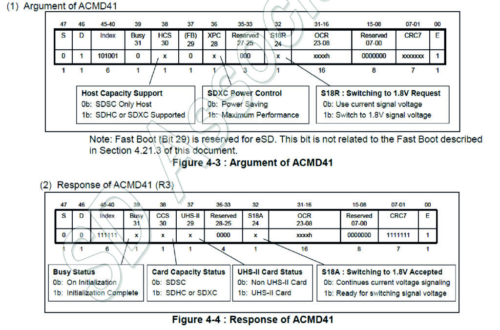
3. CMD2 (ALL_SEND_CID) : CID is a unique card ID number.
4. CMD3 (SEND_RELATIVE_ADDR) which asks the card to send it’s relative card address (RCA).
*********************************
Now to enter Data TX mode :
5. CMD7 : Puts the card into TX mode.
6. CMD18 : Multiple Block Read (continues until CMD12 STOP_TRANSMISSION)
7. DAT0 bus sends first 1 of 4 bits LOW followed by a continuous data stream synchronized with the CLK.
**************************
FTDI
I am just now thinking that if I am making a product I don’t necessarily need to worry about making it USB programmable. I can just leave the programming header and a link to how to program with Arduino/raspberry pi.
Looking in to FTDI replacements. This post (https://forum.arduino.cc/t/explanation-of-ftdi/267058/4) suggests these :
- Sil Labs CP2102
- Prolific PL2303
- WCH CH340 (Olimex has a board here : https://www.olimex.com/Products/Breadboarding/BB-CH340T/open-source-hardware)
Fabien says that these chips only do UART however. (But the NANDLAND GO board seems to have one https://nandland.com/wp-content/uploads/2022/06/Go_Board_V1.pdf)
There are some open JTAG techniques. Another option he suggests is to have a bootloader as is done with the following boards :
- tinyFPGA-BX (Uses the FPGA itself to program the flash chip : https://github.com/tinyfpga/TinyFPGA-Bootloader)
- Fomu (Uses the FPGA itself to program the flash chip : https://github.com/im-tomu/foboot)
- ICE40HX1K-EVB (Uses an Arduino board – olimexino-32u4 – to program the flash chip)
****
Saw on a blog that controlling a USB flash drive with SPI might be easier than an SD card for some reason ? It looks like a state machine is how you make an FPGA behave like a microcontroller for this type of situation.
Perhaps the usual SPI for SD card is the correct choice. Some things I’m looking at :
- https://hackaday.io/project/160928/logs
- https://www.fpga4fun.com/SPI2.html
- https://hackaday.io/project/119133-rops/log/144622-starting-with-verilog-and-spi
- SPI slave : https://github.com/joeferner/fpga-spi/blob/master/spi.v
- ***NANDLAND SPI Master : https://github.com/nandland/spi-master/blob/master/Verilog/source/SPI_Master.v***
- Optimized SPI Master: https://github.com/freecores/tiny_spi/blob/master/rtl/verilog/tiny_spi.v
- https://alchitry.com/serial-peripheral-interface-spi-verilog
The Nandland SPI Master compiles. Looking at these documents now explaining SD card protocol with SPI :
- http://www.dejazzer.com/ee379/lecture_notes/lec12_sd_card.pdf
- https://users.ece.utexas.edu/~valvano/EE345M/view12_SPI_SDC.pdf
SD interfacing with SPI :
HxD is a tool for raw SD card editing. It could help finding the start address of the first file for instance.
I think step 1 would be to try to do this manually (using an SPI library ?) with Arduino and a logic analyzer / oscilloscope to confirm that what I’m trying to do works with the particular card I am using. With screenshots of the communication I could then attempt to replicate this with the FTDI FPGA which has an SD card and LEDs for indicators.
Explaining how to use Arduino SPI library to send individual bytes :
https://docs.arduino.cc/tutorials/generic/introduction-to-the-serial-peripheral-interface/
https://docs.arduino.cc/learn/communication/spi/?_gl=1*4f5308*_ga*MTk5MjE1MjA0My4xNzA1NzQyNDIx*_ga_NEXN8H46L5*MTcxMTEzOTU0Ny4zOS4wLjE3MTExMzk1NTIuMC4wLjY5OTM2NjkyOQ..*_fplc*SVhlSkEzOXkwVlFqc2MlMkZ6ZlU5NTlzYTJteWJnTWZ5eUVlSUFDSlRZSTl3bVJHd3lMWVZiWTNFenpMUjhOOTVFR2drR3lPdU1NR0pSQWluMGRWYWZRM3htUWFBd3JYeFFiViUyQndybE1SZk9VU1JFT0Y0cXpldG5HVnZXbE1RUSUzRCUzRA..
.
****
Looking at enclosures and found these resources :
https://www.protocase.com/blog/2020/02/20/how-to-choose-between-enclosure-styles/

ponoko.com/blog/how-to-make/making-enclosures-for-electronics-with-ponoko/
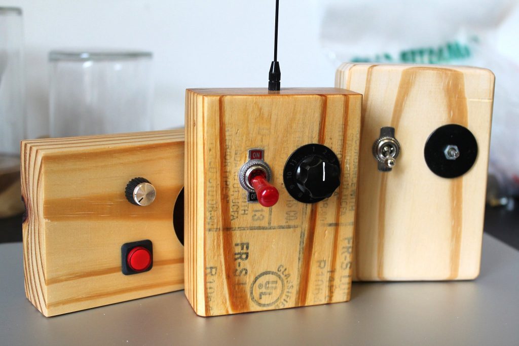


Here are some experiments with enclosures :
****
Here’s a more precise model of the 3D print option :

****
Trying to output low resolution images from film using ffmpeg (https://www.bannerbear.com/blog/how-to-extract-images-from-a-video-using-ffmpeg/):
ffmpeg -i input.mp4 -s 100x100 -vf fps=1,extractplanes=y %04d.bmp- This outputs 1 frame a second super small in black and white. The input video needs to be in the same directory of the ffmpeg.exe file. Super easy ! I renamed one of the .bmp as a .raw and opened it in photoshop at 100×100 :
- *** A couple tests using the screen itself as a display with text overlay :

 *******
- Learning about setting up multiple binary files for cold booting here https://www.latticesemi.com/support/answerdatabase/3/3/4/3344 In Diamond Programmer, Design > Utilities > Deployment Tool. You can then select Advanced SPI flash and start adding binaries and clicking next.
- After generating the .mcs file I select it as the binary input in Diamond Programmer. I wish I had added a little 2 switch DIP connected to CBSEL1, CBSEL0 so that when CRESET_B is activated you could select different images. Probably also smart to have a much bigger SPI Flash so that I could also store other types of files ? iCE40-I2C-and-SPI-Hardened-IP-User-Guide : https://www.latticesemi.com/-/media/LatticeSemi/
Documents/ApplicationNotes/IK/FPGA-TN-02010-1-8-iCE40-I2C-and-SPI-Hardened-IP-User-Guide.ashx?document_id=50480 ******** Am finally finishing the béchamel 2 with the new board :
Takes so long to assemble !
*Update* : Finished the béchamel 2 !
- With some nice flexible silicone wire I hardwired the 590 CLK with the RCLK,
- I connected VSYNC and 4040 Counter Reset to the unused board jumper pins,
- I cut the traces going from the output butter enables to the board jumper and pulled all the ENs to the ground so that all channels are displayed all the time. I did this on the backside of the board by conecting with vias.
- I put electrical tape to hold wires down and insolate bare contacts that touch when the board are stacked.
It is kinda cool ! Maybe not freezing images with sync as well as could have hoped but having the keypad definitely makes it feel “playable” and the colors and palipmsest are nice so far 🙂
Some screen shots showing the multi-color action :


Some things I am realizing about this version :
It’s possible to get the adress divisions and frequency divisions just right so that recordings stay in the same place and can be truly stacked like screen printing different layers. The idea of having a video with a clear sequence (zoom out, rotate around, pan through) and using this record and paste technique could lead to cool effects.
I also wonder if I’ve kind of reached the end of what is possible with this SRAM recording exercise. EDIT : TRY FEEDBACK LOOPING !
*EDIT* I took one pin from the VGA COLOR OUT and connected it in place of a RPI IN pin. It’s a bit hard to understand what’s happening but things get muddy quickly. When it isn’t oversaturating it gives this nice overlay (in white) effect.
Just a reminder also that this board requires some physical pressure on either the flash chip or the clock or the south end of the FPGA to get programming to work for some reason. Here is the error message :
ERROR - Function:CHECK_ID

Data Expected: h16 Actual: h1F
Found a thing that helps in Diamond Programmer : EDIT > SETTINGS >PROGRAMMING > CONTINUE DOWNLOAD ON ERROR
EDIT: I wonder if I could explore the concept of time more directly in these animations. Now that I can freeze a past frame and place it directly over a present frame, I can start to play with sequence a little. Sean Cubitt’s article about the digital image: http://www.visualfields.co.uk/Cubitt.pdf
*******
Reviewing the open source FPGA process.
1. Migen (https://m-labs.hk/gateware/migen/) is for Python to Verilo. It doesn’t look to me (http://m-labs.hk/docs/migen-tutorial.pdf) like a shortcut however…
2. IceStorm flow (https://clifford.at/icestorm) which includes Yosys, Arachne-pnr / Nextpnr, and IceStorm.
IceStorm – The core of the project, IceStorm is the part that handles the bitstream documentation and provides the tools for bitstream analysis and creation for iCE40 FPGAs.
Arachne-PNR – A place-and-route tool initially used in conjunction with IceStorm (later replaced by nextpnr).
Nextpnr – An improved and versatile place-and-route tool that has largely supplanted Arachne-PNR in the open-source FPGA community. It is designed to be a vendor-neutral, timing-driven place and route tool.
Yosys – An open-source synthesis tool for converting Verilog (a hardware description language) code into a gate-level representation that can be used with the place-and-route tools. Yosys is highly flexible and supports various synthesis tasks.
*****
What would a video workshop look like ?
CRT:
- Inputing fixed voltages, then simple waves (square, triangle, sawtooth, sine) at different frequencies. What is a Hertz ? What kind of frequencies can the eye see ? Drawing and redrawing.
- Arduino sending stored voltages.
COMPOSITE?
VGA:
- The VGA protocol and pinouts.
- Arduino generating timing signals and us sending voltages, simple waves.
- Taking a video in and switching the colors, doing some mixing and filtering.
- Using VGAX to generate different patterns based on code.
HDMI:
- The HDMI protocol and pinouts. Differential signals and the DC balanced concept.
- FPGA generating timing signals, us sending signals.
- Using Verilog to generate some simple patterns.
****
Doing some wiki surfing while watching the great series Le Temps des Ouvriers on Arte :
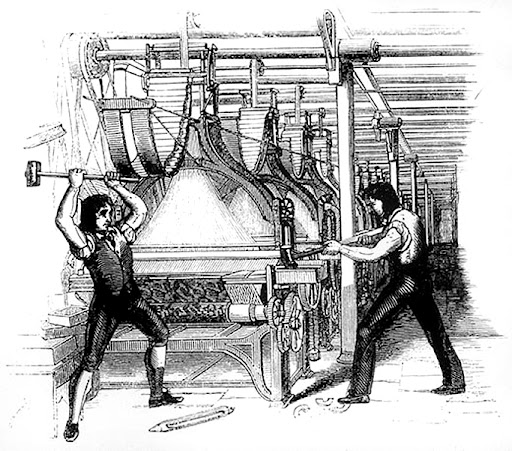
- Une perruque : An object made on company machines during company time, but for the satisfaction or purposes of the worker.
- That barricades during the Paris Commune were constructed with military precision and centrally-organized. Organic barricades were banned.
- Sabotage, window and machine breaking, la grève, taking over factories, la désobéissance.
- Detournement, découpé (cut up) as a technique for chance recombining of texts which encourages the subconscious to come to the fore.


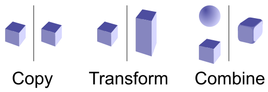
- The only creative operations are copy, transform and recombine according to Kirby Ferguson
- On this same theme, there are aparrently seven principle elements of art (https://en.wikipedia.org/wiki/Elements_of_art) : line, shape, texture, form, space, color and value, with the additions of mark making, and materiality.
- Types of cinematic transitions / cuts : https://screencraft.org/blog/everything-screenwriters-need-to-know-about-transitions/
- The experimental method involves reproducing a phenomenon and varying a single parameter related to the hypothesis to be tested.
- The various views on the filmmaking technique of montage.
**********
Serge had some advice for my project :
- Make a short text (and title!) that explains the project to someone with zero tech refs and background. Universalize the explanation, don’t get stuck in your head referencing yourself. He thinks that prepared instruments is already too much of an wink wink. He likes the water analogy.
- Keep the purism, it is the central interest of the project !! If you remove this aspect and just make an app it takes away all of the value (like switching real turn tables and actual vinyl with those fake turn table interfaces, or the Strandbeest with a motor !). The situation where the button you push “directly” influences the video signals makes video like a material medium.
Short text attempt :
A screen takes video signals in and displays them as changing colors in a window. A video cable is like a river containing signals which are like ripples in the water. This device intervenes inbetween the creation of the video signals and their display on the screen; it allows for direct manipulation of these video signals, creating loops like eddies and other kinds of turbulence, all are instantly visible on the screen.
Like a sketchpad for video !
Live video collaging machine / Live montage machine.
*****
Proposal for video workshop with DSAA / NO SCHOOL:
Start by cutting VGA cable and putting pins on a breadboard.
- What happens when you remove a color ? GND ? V or H sync ?
- How about switching colors ?
- Look at V and H sync on the oscilloscope
Let’s make waves with a function generator and see what they look like on screen.
- What do different frequencies look like on screen ?
- How about different wave types and duty cycles ?
(INCLUDE THIS?) What can we do with analog electronics ?
- A simple low-pass filter ?
- An amp
- A delay wire (just a coil of wire) ?
Get a second VGA video source.
- What happens when you mix colors from one source and colors from another source ?
- Which H and V signals do you send along to the screen ?
- Try using a potentiometer to mix two colors together, or fade a color out.
Introduction to logic:
- Let’s use a comparator to convert analog into ON or OFF
- Let’s try using an AND, OR and XOR with two video sources.
Introduction to FPGAs : The FPGA is reconfigurable logic which you can program to mess with video signals and respond to a tactile interface. To program the logic gates we use a Hardware Description Language (HDL) like verilog.
- Let’s generate a video signal using an FPGA
- Let’s generate some simple patterns
- Lets’s make it react to button touches
************
Trying to get SRAM + HDMI working together with the CC version. So far it doesn’t like using clk100 for the PLL and for always block. Also fails during placement for unknown reason.
//-----------------------------------------------------------------
// Attempt at SRAM and HDMI OUT
//-----------------------------------------------------------------

`default_nettype none // disable implicit definitions by Verilog

module top(
input wire clk100,

input wire [8:0]key,

output [3:0] hdmi_p,
output [3:0] hdmi_n,

input wire reset,

input wire r_in, //need to be soldered on the Cyber Campus board
input wire b_in, //need to be soldered on the Cyber Campus board
input wire g_in, //need to be soldered on the Cyber Campus board


output reg [17:0] addr,
inout wire [7:0] io, // inout must be type wire

output wire cs,
output wire oe,
output reg we

);

// for translating between input and output with the io pins
wire [7:0] data_in;
wire [7:0] data_out;

reg [7:0] a, b;

assign io = key[0] ? a : 8'bzzzzzzzz;

assign cs = 1;
assign oe = 1;

assign data_out = b;

assign data_in[0] = r_in;
assign data_in[1] = r_in;
assign data_in[2] = b_in;
assign data_in[3] = b_in;
assign data_in[4] = g_in;
assign data_in[5] = g_in;
assign data_in[7:6] = 2'b00;


// For holding the outward bound TMDS symbols in the slow and fast domain
reg [9:0] c0_symbol; reg [9:0] c0_high_speed;
reg [9:0] c1_symbol; reg [9:0] c1_high_speed;
reg [9:0] c2_symbol; reg [9:0] c2_high_speed;
reg [9:0] clk_high_speed;

reg [1:0] c2_output_bits;
reg [1:0] c1_output_bits;
reg [1:0] c0_output_bits;
reg [1:0] clk_output_bits;

wire clk_x5;
reg [2:0] latch_high_speed = 3'b100; // Controlling the transfers into the high speed domain

wire vsync, hsync;
wire [1:0] syncs; // To glue the HSYNC and VSYNC into the control character
assign syncs = {vsync, hsync};

// video structure constants
parameter hpixels = 800; // horizontal pixels per line
parameter vlines = 525; // vertical lines per frame
parameter hpulse = 96; // hsync pulse length
parameter vpulse = 2; // vsync pulse length
parameter hbp = 144; // end of horizontal back porch (96 + 48)
parameter hfp = 784; // beginning of horizontal front porch (800 - 16)
parameter vbp = 35; // end of vertical back porch (2 + 33)
parameter vfp = 515; // beginning of vertical front porch (525 - 10)

// registers for storing the horizontal & vertical counters
reg [9:0] vc;
reg [9:0] hc;
// generate sync pulses (active high)
assign vsync = (vc < vpulse);
assign hsync = (hc < hpulse);

always @(posedge clk_x5) begin
//-------------------------------------------------------------
// Now take the 10-bit words and take it into the high-speed
// clock domain once every five cycles.
//
// Then send out two bits every clock cycle using DDR output
// registers.
//-------------------------------------------------------------
c0_output_bits <= c0_high_speed[1:0];
c1_output_bits <= c1_high_speed[1:0];
c2_output_bits <= c2_high_speed[1:0];
clk_output_bits <= clk_high_speed[1:0];
if (latch_high_speed[2]) begin // pixel clock 25MHz
c0_high_speed <= c0_symbol;
c1_high_speed <= c1_symbol;
c2_high_speed <= c2_symbol;
clk_high_speed <= 10'b0000011111;
latch_high_speed <= 3'b000;
if (hc < hpixels)
hc <= hc + 1;
else
begin
hc <= 0;
if (vc < vlines)
vc <= vc + 1;
else
vc <= 0;
end
end
else begin
c0_high_speed <= {2'b00, c0_high_speed[9:2]};
c1_high_speed <= {2'b00, c1_high_speed[9:2]};
c2_high_speed <= {2'b00, c2_high_speed[9:2]};
clk_high_speed <= {2'b00, clk_high_speed[9:2]};
latch_high_speed <= latch_high_speed + 1'b1;
end
end

//SRAM address counter
always @(posedge clk100) begin

if (reset) begin
addr <= 0;
end

else begin
addr <= addr+1;
end

end


//REC control

always @(posedge clk100) begin

b <= io;
a <= data_in;
if (key[0]==1) begin
we <= addr[0]; //not sure why it isn't the inverse of addr[0] but that doesn't make the inverse on 'scope
end
else begin
we <= 1;
end

end

always @(*) // display 100% saturation colourbars
begin
// first check if we're within vertical active video range
if (vc >= vbp && vc < vfp)
begin
// now display different colours every 80 pixels
// while we're within the active horizontal range
// -----------------
// display white bar


if (hc >= hbp && hc < hfp)
begin
if (data_out[1:0] == 1)
begin
c2_symbol = 10'b1011110000; // red
c1_symbol = 10'b1011110000; // green
c0_symbol = 10'b1011110000; // blue
end
else
begin
c2_symbol = 10'b0111110000; // red
c1_symbol = 10'b0111110000; // green
c0_symbol = 10'b0111110000; // blue
end
end
// we're outside active horizontal range
else
begin
c2_symbol = 10'b1101010100; // red
c1_symbol = 10'b1101010100; // green
//---------------------------------------------
// Channel 0 carries the blue pixels, and also
// includes the HSYNC and VSYNCs during
// the CTL (blanking) periods.
//---------------------------------------------
case (syncs)
2'b00 : c0_symbol = 10'b1101010100;
2'b01 : c0_symbol = 10'b0010101011;
2'b10 : c0_symbol = 10'b0101010100;
default : c0_symbol = 10'b1010101011;
endcase
end
end
// we're outside active vertical range
else
begin
c2_symbol = 10'b1101010100; // red
c1_symbol = 10'b1101010100; // green
//---------------------------------------------
// Channel 0 carries the blue pixels, and also
// includes the HSYNC and VSYNCs during
// the CTL (blanking) periods.
//---------------------------------------------
case (syncs)
2'b00 : c0_symbol = 10'b1101010100;
2'b01 : c0_symbol = 10'b0010101011;
2'b10 : c0_symbol = 10'b0101010100;
default : c0_symbol = 10'b1010101011;
endcase
end
end

// red N
defparam hdmin2.PIN_TYPE = 6'b010000;
defparam hdmin2.IO_STANDARD = "SB_LVCMOS";
SB_IO hdmin2 (
.PACKAGE_PIN (hdmi_n[2]),
.CLOCK_ENABLE (1'b1),
.OUTPUT_CLK (clk_x5),
.OUTPUT_ENABLE (1'b1),
.D_OUT_0 (~c2_output_bits[1]),
.D_OUT_1 (~c2_output_bits[0])
);

// red P
defparam hdmip2.PIN_TYPE = 6'b010000;
defparam hdmip2.IO_STANDARD = "SB_LVCMOS";
SB_IO hdmip2 (
.PACKAGE_PIN (hdmi_p[2]),
.CLOCK_ENABLE (1'b1),
.OUTPUT_CLK (clk_x5),
.OUTPUT_ENABLE (1'b1),
.D_OUT_0 (c2_output_bits[1]),
.D_OUT_1 (c2_output_bits[0])
);

// green N
defparam hdmin1.PIN_TYPE = 6'b010000;
defparam hdmin1.IO_STANDARD = "SB_LVCMOS";
SB_IO hdmin1 (
.PACKAGE_PIN (hdmi_n[1]),
.CLOCK_ENABLE (1'b1),
.OUTPUT_CLK (clk_x5),
.OUTPUT_ENABLE (1'b1),
.D_OUT_0 (~c1_output_bits[1]),
.D_OUT_1 (~c1_output_bits[0])
);

// green P
defparam hdmip1.PIN_TYPE = 6'b010000;
defparam hdmip1.IO_STANDARD = "SB_LVCMOS";
SB_IO hdmip1 (
.PACKAGE_PIN (hdmi_p[1]),
.CLOCK_ENABLE (1'b1),
.OUTPUT_CLK (clk_x5),
.OUTPUT_ENABLE (1'b1),
.D_OUT_0 (c1_output_bits[1]),
.D_OUT_1 (c1_output_bits[0])
);


// blue N
defparam hdmin0.PIN_TYPE = 6'b010000;
defparam hdmin0.IO_STANDARD = "SB_LVCMOS";
SB_IO hdmin0 (
.PACKAGE_PIN (hdmi_n[0]),
.CLOCK_ENABLE (1'b1),
.OUTPUT_CLK (clk_x5),
.OUTPUT_ENABLE (1'b1),
.D_OUT_0 (~c0_output_bits[1]),
.D_OUT_1 (~c0_output_bits[0])
);

// blue P
defparam hdmip0.PIN_TYPE = 6'b010000;
defparam hdmip0.IO_STANDARD = "SB_LVCMOS";
SB_IO hdmip0 (
.PACKAGE_PIN (hdmi_p[0]),
.CLOCK_ENABLE (1'b1),
.OUTPUT_CLK (clk_x5),
.OUTPUT_ENABLE (1'b1),
.D_OUT_0 (c0_output_bits[1]),
.D_OUT_1 (c0_output_bits[0])
);

// clock N
defparam hdmin3.PIN_TYPE = 6'b010000;
defparam hdmin3.IO_STANDARD = "SB_LVCMOS";
SB_IO hdmin3 (
.PACKAGE_PIN (hdmi_n[3]),
.CLOCK_ENABLE (1'b1),
.OUTPUT_CLK (clk_x5),
.OUTPUT_ENABLE (1'b1),
.D_OUT_0 (~clk_output_bits[1]),
.D_OUT_1 (~clk_output_bits[0])
);


// clock P
defparam hdmip3.PIN_TYPE = 6'b010000;
defparam hdmip3.IO_STANDARD = "SB_LVCMOS";
SB_IO hdmip3 (
.PACKAGE_PIN (hdmi_p[3]),
.CLOCK_ENABLE (1'b1),
.OUTPUT_CLK (clk_x5),
.OUTPUT_ENABLE (1'b1),
.D_OUT_0 (clk_output_bits[1]),
.D_OUT_1 (clk_output_bits[0])
);
// D_OUT_0 and D_OUT_1 swapped?
// https://github.com/YosysHQ/yosys/issues/330


SB_PLL40_PAD #(
.FEEDBACK_PATH ("SIMPLE"),
.DIVR (4'b0000),
.DIVF (7'b0001001),
.DIVQ (3'b011),
.FILTER_RANGE (3'b101)
) uut (
.RESETB (1'b1),
.BYPASS (1'b0),
.PACKAGEPIN (clk100),
.PLLOUTGLOBAL (clk_x5) // DVI clock 125MHz
);

endmodule
set_io hdmi_p[0] 139 -io_std SB_LVCMOS
set_io hdmi_p[2] 78 -io_std SB_LVCMOS
set_io hdmi_p[1] 80 -io_std SB_LVCMOS
set_io hdmi_p[3] 137 -io_std SB_LVCMOS
set_io hdmi_n[0] 138 -io_std SB_LVCMOS
set_io hdmi_n[2] 79 -io_std SB_LVCMOS
set_io hdmi_n[1] 81 -io_std SB_LVCMOS
set_io hdmi_n[3] 136 -io_std SB_LVCMOS

set_io key[0] 37
set_io key[1] 38
set_io key[2] 39
set_io key[3] 41
set_io key[4] 42
set_io key[5] 43
set_io key[6] 44
set_io key[7] 45
set_io key[8] 47

set_io SCK 32

set_io CMD 33

set_io LED1 29

set_io LED5 28

set_io reset 66

set_io clk100 49

set_io v_sync 97

set_io h_sync 76

set_io io[0] 7
set_io io[1] 8
set_io io[2] 9
set_io io[3] 10
set_io io[4] 11
set_io io[5] 12
set_io io[6] 19
set_io io[7] 22

set_io addr[0] 4
set_io addr[1] 3
set_io addr[2] 2
set_io addr[3] 1
set_io addr[4] 144
set_io addr[5] 143
set_io addr[6] 142
set_io addr[7] 141
set_io addr[8] 120
set_io addr[9] 121
set_io addr[10] 24
set_io addr[11] 122
set_io addr[12] 135
set_io addr[13] 119
set_io addr[14] 134
set_io addr[15] 116
set_io addr[16] 129
set_io addr[17] 128

set_io cs 25

set_io oe 23

set_io we 118
set_io r_in 52
set_io g_in 58
set_io b_in 63